Optical modulating device having gate structure

An optical modulation, photonic nanotechnology, applied in optics, nano-optics, optical components, etc., can solve problems such as slow operation response time

Active Publication Date: 2017-09-26
SAMSUNG ELECTRONICS CO LTD +1
View PDF5 Cites 10 Cited by
  • Summary
  • Abstract
  • Description
  • Claims
  • Application Information

AI Technical Summary

Problems solved by technology

However, the operational response time of such optical modulators is slow and can reach several μs according to known methods of driving optical modulators.

Method used


Image

  • Optical modulating device having gate structure
  • Optical modulating device having gate structure
  • Optical modulating device having gate structure

Examples


Embodiment Construction

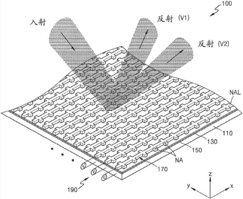
[0031] One or more exemplary embodiments may provide optical devices that modulate light.

[0032] Additional exemplary aspects will be set forth in part in the description which follows and, in part, will be obvious from the description, or may be learned by practice of the exemplary embodiments.

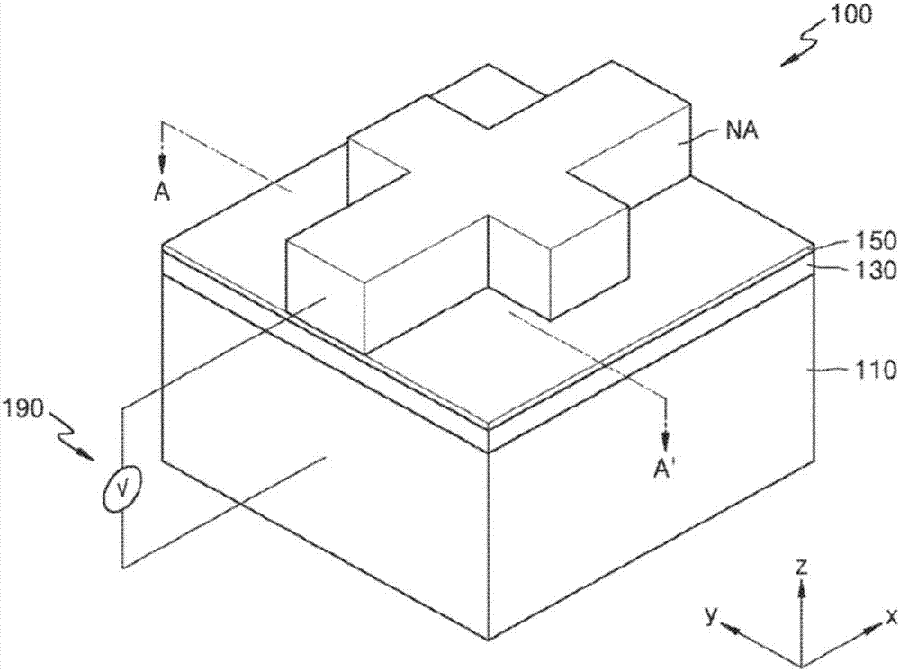
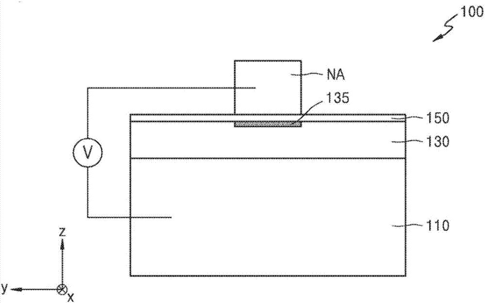
[0033] According to an aspect of the exemplary embodiment, the optical modulation device includes a plasmonic nanoantenna layer; a metal layer facing the plasmonic nanoantenna layer; a permittivity change layer between the plasmonic nanoantenna layer and the metal layer, the The permittivity change layer has a permittivity that varies according to a signal applied thereto; and a dielectric material layer between the plasmonic nanoantenna layer and the metal layer.

[0034] The optical modulation device may further include: a signal applying device configured to apply a signal to the permittivity change layer, thereby causing a change in permittivity of the permittivity change layer...


PUM


Abstract

An optical modulation device includes a plasmonic nano-antenna layer, a metal layer that faces the plasmonic nano-antenna layer, and a permittivity variation layer and a dielectric material layer between the plasmonic nano-antenna layer and the metal layer. An active area formed in the permittivity variation layer according to an external signal may function as a gate that controls optical modulation performance.

Description

technical field [0001] Apparatuses consistent with exemplary embodiments relate to optics for modulating light. Background technique [0002] Optical devices that change the transmittance, reflection, polarization, phase, intensity, path, etc. of incident light are used in various optical devices. Optical modulators used in optical systems have various structures for controlling these properties in a desired manner. [0003] As examples, anisotropic liquid crystal and microelectromechanical systems (MEMS) structures that use micromechanical motion to block light or control reflective elements and other elements are widely used in typical optical modulators. However, the operational response time of such optical modulators is slow and can reach several μs according to known methods of driving optical modulators. [0004] It is desirable to utilize nanoantennas in conjunction with optical modulators, which exploit the phenomenon of surface plasmon resonance that occurs at th...

Claims


Application Information

Patent Timeline
Patent Type & Authority Applications(China)
IPC IPC(8): G02F1/29G02F1/00G02F1/01G02B5/00B82Y20/00
CPCB82Y20/00G02B5/008G02F1/0018G02F1/01G02F1/292G02F2203/11G02F2203/10G02F2203/50G02F2202/30
Inventor 韩承勋黄耀纬H.A.阿特沃特李浩玮R.索科彦G.帕帕达基斯K.特亚加拉詹
Owner SAMSUNG ELECTRONICS CO LTD
Why Eureka
Try Eureka