

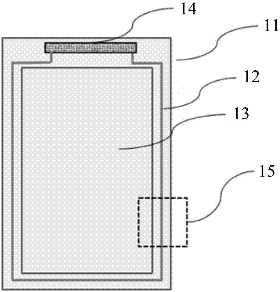
Array substrate
A technology of array substrates and polar plates, which is applied in nonlinear optics, instruments, optics, etc., can solve the problems of weakening the anti-static impact ability of products and compressing wiring space, etc.
- Summary
- Abstract
- Description
- Claims
- Application Information
AI Technical Summary
Problems solved by technology
Method used
Image

Examples
Embodiment 1
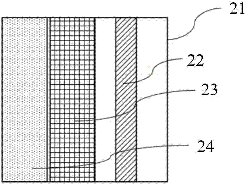
[0057] by Figure 4 The protected area is cut at the position shown by AA`, and the film layer structure of the protected area of the array substrate in this embodiment is as follows: Figure 5 Show, Figure 5 Middle 56 is the bottom substrate, generally made of glass, and can also be made of organic plastic. 55 is the buffer layer, which is generally made of SiO2 film and SiNx film, and the SiO2 film thickness is SiNx film thickness is 54 is the gate insulation layer, generally made of SiO2, with a thickness of 53 is the interlayer dielectric layer (ILD layer), which is generally made of SiO2 film and SiNx film, and the thickness of the two films is 52 is a planarization layer (PLN layer), and its thickness is generally The function of the planarization layer in the display area is mainly to isolate the interference between the pixel electrode layer (ITO) and the data line. 51 is a protective layer (PV layer), generally made of SiNx, with a thickness of In the ...
Embodiment 2
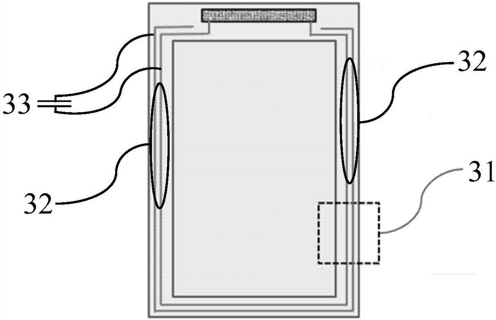
[0075] The film layer structure of this embodiment is as Figure 9 As shown, the planar structure diagram of each film layer is shown in Figures 10a-10c shown. The structure and characteristics of each film layer in this embodiment can refer to Embodiment 1, and will not be repeated here. Further, as Figure 9 and Figure 10a As shown, 101 is the first wiring, and 102 is the first part of the second wiring (a part of the second wiring), both of which are formed by the third metal layer L3. The width of the first wiring 101 and the first part of the wiring 102 is preferably 10-30 μm, the distance between the first wiring 101 and the first part of the wiring 102 is preferably 5-10 μm, and the distance between the first part of the wiring 102 and the edge of the array substrate The distance is preferably 20-80 μm.
[0076] The difference between this embodiment and Embodiment 1 is that the second part of the second routing 103 (another part of the second routing) is formed ...
Embodiment 3
[0084] The film layer structure of this embodiment is as Figure 13 As shown, the planar structure of each film layer is as follows Figure 14a , 14b shown. The structure and characteristics of each film layer in this embodiment can refer to Embodiment 1, and will not be repeated here.
[0085] Such as Figure 13 and Figure 14a As shown, 141 is a first wiring, 142 is a second wiring, both of which are formed by the third metal layer L3. The width of the first wiring 141 and the second wiring 142 is preferably 10-30 μm, the distance between the second wiring 142 and the edge of the array substrate is preferably 20-80 μm, and the distance between them is preferably 5-10 μm.
[0086] Such as Figure 14b As shown, the second metal layer L2 is used to form the first metal region with a specific pattern. The first metal area includes a plurality of first electrode lead wires 143 and a plurality of second electrode lead wires 144 connected to the first electrode lead wires 14...
PUM
| Property | Measurement | Unit |
|---|---|---|
| width | aaaaa | aaaaa |
Abstract
Description
Claims
Application Information