A vco bias circuit with anti-single event effect function

An anti-single event effect and bias circuit technology, which is applied in logic circuits, electrical components, reliability improvement and modification, etc., can solve the problems of low anti-radiation ability, limited anti-radiation performance, and circuit anti-radiation ability Small problems, to achieve the effect of improving the radiation resistance performance

Active Publication Date: 2020-12-22
NAT UNIV OF DEFENSE TECH
View PDF9 Cites 0 Cited by
  • Summary
  • Abstract
  • Description
  • Claims
  • Application Information

AI Technical Summary

Problems solved by technology

[0003] In order to improve the anti-radiation performance of the VCO bias circuit, one method is to improve the existing process. For example, Chinese patent application (200510029396) discloses a field-effect transistor anti-radiation reinforcement method based on silicon on insulator. The device level can improve the radiation resistance of the circuit to a certain extent by reducing the back channel leakage current caused by radiation, but the effect of the overall radiation resistance of the circuit is still small, and the improvement of the existing process will be extremely harmful. The design cost is greatly increased; another method is to use double bias circuit technology, which can effectively improve the anti-radiation performance, but in the existing double bias circuit, the load resistance bias voltage generation circuit and the tail current circuit bias Therefore, it is still limited to improve the anti-radiation performance of the VCO bias circuit, especially for the impact of high-energy particles with large energy. The double-bias VCO is only comparable to the anti-radiation ability of the original VCO quite
[0004] like figure 1 The VCO dual bias circuit shown includes switches M1, M2 and differential amplifier A1, the output voltage V bisa_p with V bias_b Provide bias voltage for the load resistance and tail current circuit in the VCO oscillation loop respectively, that is, the bias voltage V is generated by the switching tubes M1 and M2 bisa_p As the load resistor bias voltage, the bias voltage V bisa_p and differential amplifier A1 to generate the bias voltage V bias_b As the bias voltage of the tail current circuit; when high-energy particles bombard the drain of the switch tube M1 or M2, a pulse current will be generated to cause V bisa_p Voltage fluctuations, the voltage fluctuations will not only directly affect the working state of the VCO oscillation loop, but also cause V through the differential amplifier A1 bias_b Voltage fluctuations, which further affect the working state of the VCO oscillation loop, and the ability to resist radiation is still not high

Method used


Image

  • A vco bias circuit with anti-single event effect function
  • A vco bias circuit with anti-single event effect function
  • A vco bias circuit with anti-single event effect function

Examples


Embodiment 1

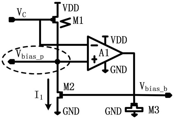
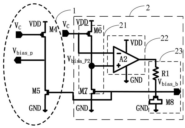
[0035] In this embodiment, the VCO bias circuit with anti-single event effect function is as follows: image 3 As shown, the first switching tube unit 11 includes a first switching tube M4 and a second switching tube M5, the gate of the first switching tube M4 is connected to the control voltage Vc, the source is connected to the power supply VDD, and the source of the second switching tube M5 Grounded, the drain of the first switch M4 is connected to the drain of the second switch M5 to generate the first bias voltage V for the load resistor bias_p The second switching tube unit 21 includes a third switching tube M6 and a fourth switching tube M7, the gate of the third switching tube M6 is connected to the control voltage Vc, the source is connected to the power supply VDD, the source of the fourth switching tube M7 is grounded, and the third switching tube M6 is connected to the power supply VDD. The drain of the third switch M6 is connected to the drain of the fourth switch...

Embodiment 2

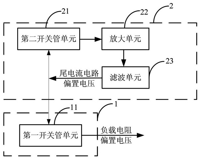
[0041] Such as Figure 5 As shown, this embodiment is basically the same as Embodiment 1, except that the first switching tube unit 11 in the load resistance bias module 1 includes two switching branches, and each switching branch includes two switching tubes connected to each other. , and one of the switch tubes is connected to the control power supply terminal, and the other switch tube is connected to the second bias voltage fed back by the tail current circuit bias module 2. The structure of each switch branch is specifically the same as that of the load resistance bias module in Embodiment 1. 1 The circuit structure is the same, and the two switching branches are connected through the first filter unit 12 to output the first bias voltage V bias_p .

[0042] Such as Figure 5 As shown, the first filtering unit 12 of this embodiment includes two resistors R and capacitor C, one end of the two resistors R is respectively connected to a switch branch, and the other end is c...


PUM


Abstract

The invention discloses a VCO bias circuit with a single event effect prevention function. The VCO bias circuit comprises a load resistance bias module and a tail current circuit bias module, wherein the load resistance bias module generates a first bias voltage through a first switching tube unit and outputs the first bias voltage to a load resistor in a VCO loop, the tail current circuit bias module generates a second bias voltage through a second switching tube unit, outputs the second bias voltage to a tail current circuit in the VCO loop, and respectively feeds back the second bias voltage to the first switching tube unit and second switching tube unit. The VCO bias circuit has the single event effect prevention function, and has the advantages of simple structure, low cost, strong radiation resistance and so on.

Description

technical field [0001] The invention relates to the technical field of integrated circuits, in particular to a VCO bias circuit suitable for a phase-locked loop with anti-single event effect function. Background technique [0002] With the rapid development of aerospace and aviation and the continuous reduction of the size of integrated circuit technology, the impact of radiation effects on the working status of electronic systems is becoming more and more severe, and may even lead to system collapse. The phase-locked loop (PLL) in the analog circuit is one of the key parts, which provides the required clock signal for the entire circuit system, and the voltage-controlled oscillation (VCO) in the phase-locked loop is the part that generates the clock, and its resistance to SET (Single Event Transient, single event transient) performance will directly affect the output clock. In the VCO, the radiation sensitivity of its bias circuit part is more serious. The bias circuit wil...

Claims


Application Information

Patent Timeline
Patent Type & Authority Patents(China)
IPC IPC(8): H03K19/003
CPCH03K19/00338
Inventor 郭阳郭前程梁斌胡春媚陈建军陈希袁珩洲
Owner NAT UNIV OF DEFENSE TECH
Why Eureka
Try Eureka