Method for processing single-face wire embedding printed circuit board without core board

A technology for printed circuit boards and processing methods, which is applied in the fields of printed circuit, printed circuit manufacturing, and multilayer circuit manufacturing. Major problems, to achieve the effect of improving the yield rate

Active Publication Date: 2017-10-10
SHANGHAI MEADVILLE SCI & TECH
View PDF2 Cites 10 Cited by
  • Summary
  • Abstract
  • Description
  • Claims
  • Application Information

AI Technical Summary

Problems solved by technology

Since the embedding carrier board itself is made of carrier copper foil reverse pressure, the outermost layer of ultra-thin copper foil is easily damaged and easily corroded. This process requires 5 processes on the carrier board for edge sealing. The yield rate of mass processing of products has a great impact

Method used


Image

  • Method for processing single-face wire embedding printed circuit board without core board
  • Method for processing single-face wire embedding printed circuit board without core board
  • Method for processing single-face wire embedding printed circuit board without core board

Examples


Embodiment Construction

[0033] The present invention will be further described below in conjunction with the embodiments and accompanying drawings.

[0034] see Figure 1-Figure 12 , the manufacturing method of the coreless board single-sided embedding printed circuit board of the present invention, the main manufacturing process is as follows:

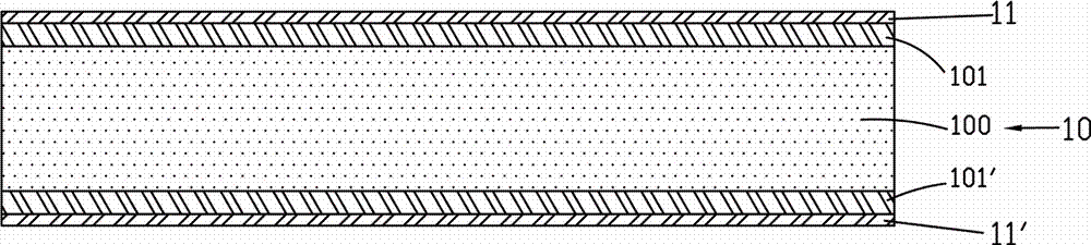
[0035] 1) Paste two first copper foils 11, 11' with a thickness of 3 μm on the carrier board 10 with an adhesive on the smooth side to obtain a processed board whose thickness and rigidity can meet the processing requirements of ordinary equipment. Sectional diagram as figure 1 As shown; in this embodiment, the carrier 10 is composed of two copper foils 101, 101' with a thickness of 17 μm and a core 100, and the core 100 is made of PP (polypropylene) material.

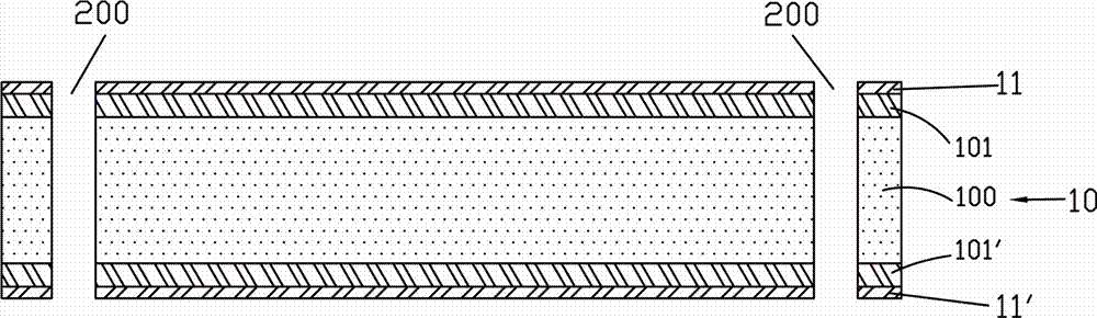
[0036] 2) Drill a row of mechanical through holes 200 along the periphery of the edge of the processed plate formed in step 1) according to the hole center distance of 5 mm and the hole diameter of...


PUM


Abstract

The invention provides a method for processing a single-face wire embedding printed circuit board without a core board. The method comprises the following steps: coating two ultrathin copper foils on a carrier board to obtain a processing board, and drilling a certain number of mechanical through holes in the edge area of the processing board; manufacturing a wire embedding layer circuit on the surface of the cooper foils of the processing board through an addition method, and meanwhile metalizing the mechanical through holes; increasing layers by using conventional printed circuit board processing flow, wherein the metalized mechanical through holes on the board edge are filled by an insulated dielectric material; and in a subsequent processing course, the metalized mechanical through holes in the edge of the processing board and filled with resin protect the whole non-dismounted wire embedding board, the mechanical drilling area on the board edge is removed in an edge milling manner and is split to obtain the printed circuit board without the core board, the defect that the copper foils and the carrier board are separated easily is overcome, and mass production can be realized.

Description

technical field [0001] The present invention relates to a method for manufacturing a printed circuit board, in particular to a method for processing a printed circuit board with single-side embedding of a coreless board, and more particularly to a method for manufacturing a printed circuit board using a coreless board embedding process . Background technique [0002] With the vigorous development of the electronic industry, electronic products have entered the stage of functional and intelligent research and development. In order to meet the development needs of high integration, miniaturization and miniaturization of electronic products, printed circuit boards or semiconductor integrated circuit packaging substrates are used in Under the premise of satisfying the good electrical and thermal performance of electronic products, it is also developing towards the design trend of light, thin, short and small. At the same time, the design requirements for electronic systems are ...

Claims


Application Information

Patent Timeline
Patent Type & Authority Applications(China)
IPC IPC(8): H05K3/46
CPCH05K3/4644H05K2203/1572
Inventor 雍慧君常明陈明明李雪理
Owner SHANGHAI MEADVILLE SCI & TECH
Why Eureka
Try Eureka