Pixel circuit, driving method thereof, display panel and display device

A pixel circuit and drive control technology, applied in the field of display panels, display devices, and pixel circuits, can solve the problem of inconsistent brightness of the first frame, and achieve the effect of avoiding afterimage phenomenon, consistent brightness, and avoiding differences

Active Publication Date: 2017-10-17
WUHAN TIANMA MICRO ELECTRONICS CO LTD
View PDF12 Cites 47 Cited by
  • Summary
  • Abstract
  • Description
  • Claims
  • Application Information

AI Technical Summary

Problems solved by technology

[0004] Embodiments of the present invention provide a pixel circuit, its driving method, a display panel, and a display device, which are used to improve the afterimage existing in the existing pixel circuit and the problem of inconsistency in brightness of the first frame after switching between high and low gray scales

Method used


Image

  • Pixel circuit, driving method thereof, display panel and display device
  • Pixel circuit, driving method thereof, display panel and display device
  • Pixel circuit, driving method thereof, display panel and display device

Examples


example 1

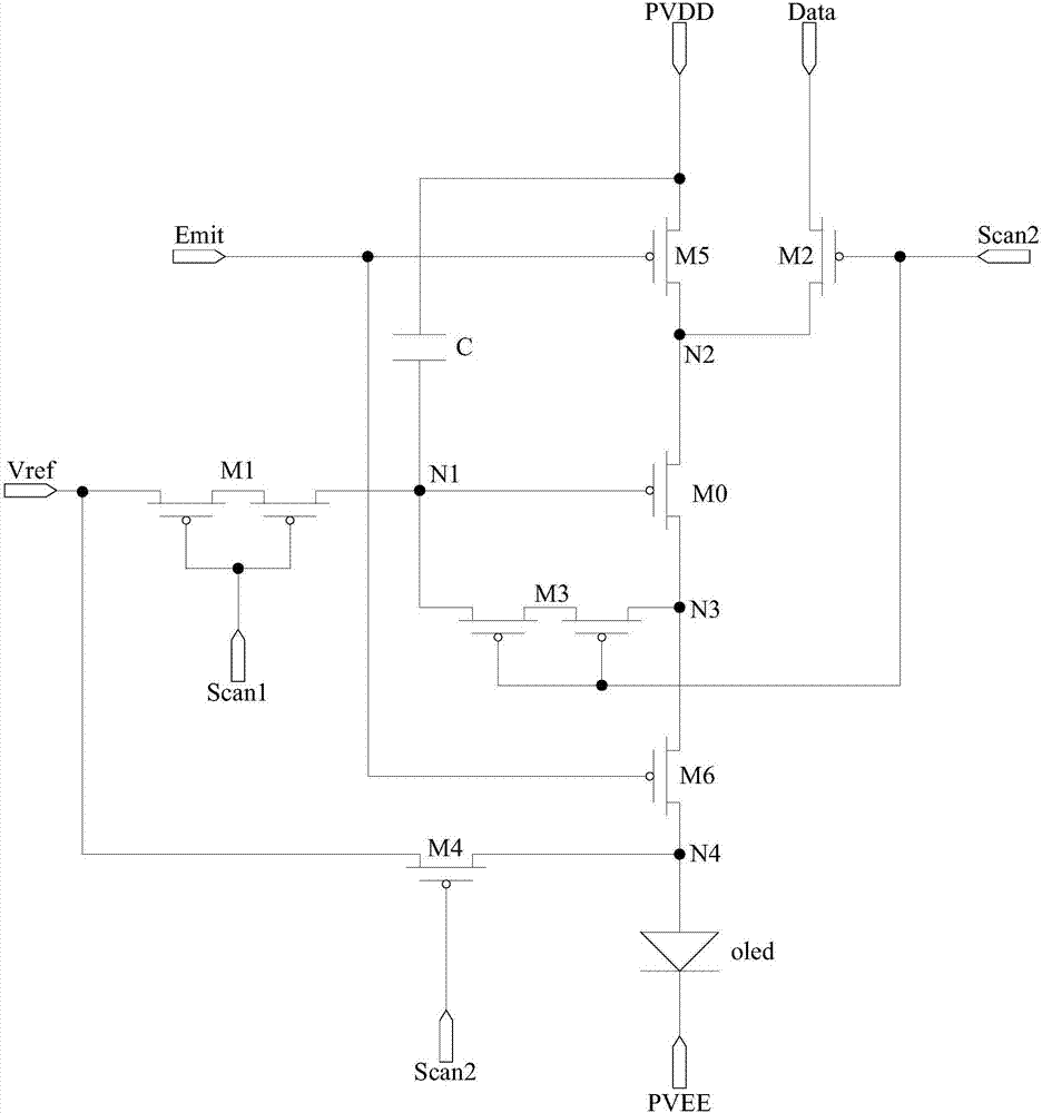
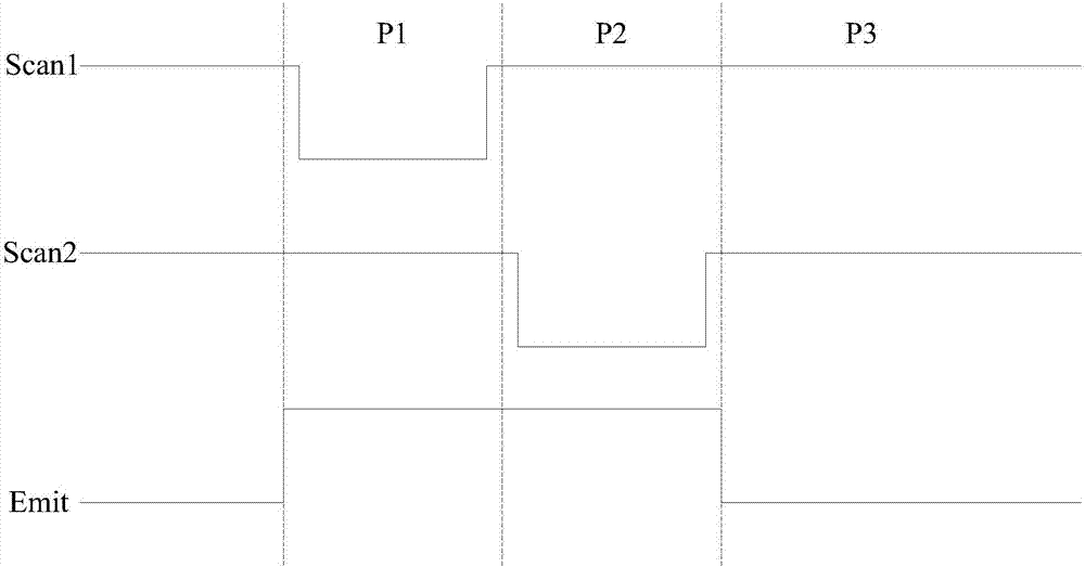
[0104] by Figure 4 Take the pixel circuit shown as an example, and the corresponding input and output timings are as follows Figure 11a shown. Specifically, choose the Figure 11a The four stages T1, T2, T3 and T4 in the input timing diagram shown.

[0105] In node initialization phase T1, Scan1=0, Scan2=1, Emit1=1, Emit2=0.

[0106] Since Scan1=0, the fifth switching transistor M5 is turned on to provide the signal of the reference signal terminal Vref to the first node N1, and the potential of the first node N1 is Vref. Since Emit2=0, the first switching transistor M1 is turned on to provide the signal of the first voltage terminal PVDD to the second node N2, the potential of the second node N2 is VDD, and the first node N1 and the second node N2 are initially reset. Since Scan2=1, the third switching transistor M3, the fourth switching transistor M4 and the sixth switching transistor M6 are turned off. Since Emit1=1, the second switching transistor M2 is turned off, ...

example 2

[0117] by Figure 5 and Figure 8 Take the pixel circuit shown as an example, and the corresponding input and output timings are as follows Figure 12 shown. Specifically, choose the Figure 12 The four stages T1, T2, T3 and T4 in the input timing diagram shown.

[0118] In node initialization phase T1, Scan1=0, Scan2=1, Emit1=Emit2=1.

[0119]Since Scan1=0, the fifth switch transistor M5 is turned on to provide the signal of the reference signal terminal Vref to the first node N1, and the potential of the first node N1 is Vref; the seventh switch transistor M7 is turned on to supply the signal of the first voltage terminal The signal of PVDD is provided to the second node N2, the potential of the second node N2 is VDD, the first node N1 and the second node N2 are initialized and reset, and the driving transistor M0 is turned on. Since Scan2=1, the third switching transistor M3, the fourth switching transistor M4 and the sixth switching transistor M6 are turned off. Sinc...

example 3

[0128] by Figure 6 , Figure 7 , Figure 9 and Figure 10 Take the pixel circuit shown as an example, and the corresponding input and output timings are as follows Figure 13 shown. Specifically, choose the Figure 13 The three stages T1, T2 and T3 in the input timing diagram are shown.

[0129] In node initialization phase T1, Scan1=0, Scan2=1, Emit1=Emit2=1.

[0130] Since Scan1=0, the fifth switch transistor M5 is turned on to provide the signal of the reference signal terminal Vref to the first node N1, and the potential of the first node N1 is Vref; the seventh switch transistor M7 is turned on to supply the signal of the first voltage terminal The signal of PVDD is provided to the second node N2, the potential of the second node N2 is VDD, the first node N1 and the second node N2 are initialized and reset, the eighth transistor is turned on and the signal of the reference signal terminal Vref is provided to the third node N3, The driving transistor M0 is turned o...


PUM


Abstract

The present invention discloses a pixel circuit, a driving method thereof, a display panel and a display device. According to the present invention, before a light-emitting device emits light, an initialization module provides the signals at a reference signal end to the grid and the second pole of a driving transistor separately, provides a signal at a first voltage end to the first pole of the driving transistor, and is utilized to reset the grid and the first pole of the driving transistor separately, so that the difference caused by the parasitic capacitances of the grid and the first pole is avoided, and further the problem that due to the voltage jump, the threshold values are captured inconsistently, is avoided, and accordingly, the consistent brightness of a first frame after the high and low gray-scale switching can be guaranteed. Moreover, the second pole of the driving transistor is reset at the initialization stage of each frame, so that a large current flows through the driving transistor, and the threshold-voltage excursion of the driving transistor caused by the bias stress is forced to recover, and accordingly, a persistence of vision phenomenon is avoided.

Description

technical field [0001] The invention relates to the field of display technology, in particular to a pixel circuit, a driving method thereof, a display panel and a display device. Background technique [0002] Organic Light Emitting Diode (OLED) is one of the hot spots in the field of flat panel display research today. Compared with liquid crystal displays, OLED has the advantages of low energy consumption, low production cost, self-illumination, wide viewing angle and fast response speed. , OLEDs have begun to replace traditional Liquid Crystal Displays (LCDs) in the field of flat panel displays such as mobile phones, PDAs, and digital cameras. Among them, pixel circuit design is the core technical content of OLED display, which has important research significance. [0003] The structure of an existing pixel circuit is as follows figure 1 As shown, it includes 6 switch transistors: M1-M6, 1 drive transistor M0 and 1 capacitor C. The corresponding input timing diagram is a...

Claims


Application Information

Patent Timeline
Patent Type & Authority Applications(China)
IPC IPC(8): G09G3/3266G09G3/3233G09G3/3208
CPCG09G3/3208G09G3/3233G09G3/3266
Inventor 高娅娜向东旭朱仁远李玥陈泽源蔡中兰
Owner WUHAN TIANMA MICRO ELECTRONICS CO LTD
Why Eureka
Try Eureka