Exposure method and exposure device

An exposure method and an exposure device technology, which are applied in photolithography exposure devices, microlithography exposure equipment, optics, etc., can solve problems such as inaccurate film thickness control and inability to perform process debugging, and improve mass production yield, Effect of reducing film thickness error and increasing process window

Active Publication Date: 2017-10-27
TCL CHINA STAR OPTOELECTRONICS TECH CO LTD
View PDF9 Cites 2 Cited by
  • Summary
  • Abstract
  • Description
  • Claims
  • Application Information

AI Technical Summary

Problems solved by technology

[0004] In view of this, the present invention provides an exposure method and an exposure device, which can solve the problems of inaccurate film thickness control and inability to perform process debugging in the prior art

Method used


Image

  • Exposure method and exposure device
  • Exposure method and exposure device
  • Exposure method and exposure device

Examples


Embodiment Construction

[0021] The following will clearly and completely describe the technical solutions in the embodiments of the present invention with reference to the drawings in the embodiments of the present invention. Apparently, the described embodiments are some, not all, embodiments of the present invention. Based on the embodiments of the present invention, all other embodiments obtained by persons of ordinary skill in the art without making creative efforts shall fall within the protection scope of the present invention.

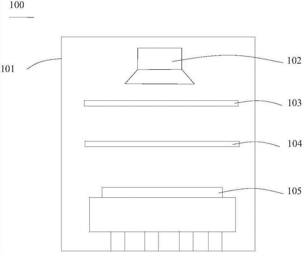
[0022] An embodiment of the present invention provides an exposure device, which is used to expose a photoresist on a substrate to form a film with a step difference. The exposure device includes but is not limited to an exposure machine.

[0023] Such as figure 1 As shown, the exposure device 100 may include a body 101, a light source 102 installed on the body 101, a filter cover 104, and n filters, figure 1 Only the filter 103 is illustrated in . Wherein, the mai...


PUM

PropertyMeasurementUnit
wavelengthaaaaaaaaaa

Abstract

The invention provides an exposure method. The exposure method is used for exposing a photoresist on a substrate to form a layer structure with a segment difference. The exposure method comprises the following steps: providing a light source, a light filtering hood and n light filters, wherein a light-impermeable area and a light filtering area are arranged on the light filtering hood, the light filtering area is used for transmitting at least two types of light rays, each light filter is used for transmitting one type of light rays, the types of the light rays transmitted by the n light filters are different from one another, and n is greater than or equal to 2; using the light source for sequentially irradiating the n light filters; sequentially using the n light filters for transmitting the light rays; performing n times exposure on the photoresist through the light filtering hood. The invention further provides an exposure device. Through the exposure method and the exposure device, film thickness control can be refined, reduction in a film thickness error is facilitated, debugging of an exposure process is facilitated, a process window is increased, and the yield rate during batch production is increased.

Description

technical field [0001] The invention relates to the technical field of liquid crystal displays, in particular to an exposure method and an exposure device. Background technique [0002] In the manufacturing process of the liquid crystal display panel, it is necessary to use a photolithography process to form a thin film on the substrate. The photolithography process includes an exposure process, and the final film thickness is different if the exposure amount is different. [0003] Actual products often require that the film thickness to be formed have several steps. In the prior art, a semi-transparent mask is often used to manufacture a thin film with a step difference in film thickness. There are several regions with different light transmittances on the translucent mask. The amount of light passing through the regions with different light transmittances is different, and the exposure amount of corresponding positions on the photoresist is also different, thus forming a...

Claims


Application Information

Patent Timeline
Patent Type & Authority Applications(China)
IPC IPC(8): G03F7/20G03F7/00G03F1/00
CPCG03F1/00G03F7/0007G03F7/2002G03F7/2004G03F7/2022
Inventor 邓金全
Owner TCL CHINA STAR OPTOELECTRONICS TECH CO LTD
Why Eureka
Try Eureka