

AMOLED pixel drive circuit
A technology of pixel drive circuit and electric potential, which is applied in instruments, static indicators, etc., can solve the problems of threshold voltage drift and affect the uniformity of panel brightness, etc., and achieve the effect of electrical drift compensation
- Summary
- Abstract
- Description
- Claims
- Application Information
AI Technical Summary
Problems solved by technology
Method used
Image

Examples
Embodiment Construction
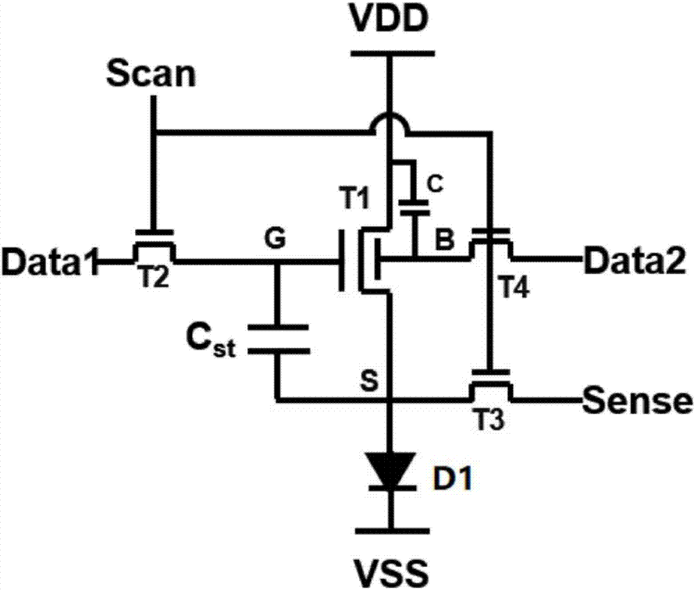
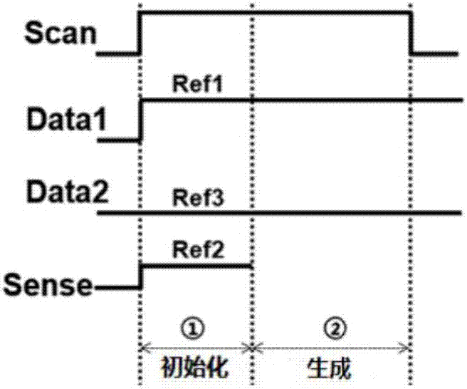
[0033] see figure 2 , in order to realize the compensation and driving of a single pixel, the present invention introduces a double-gate structure to regulate and control the threshold voltage of the driving TFT. A preferred embodiment of the AMOLED pixel driving circuit of the present invention mainly includes: a double-gate thin film transistor T1 as a driving transistor, composed of The signal of the scanning line Scan controls the thin film transistor T2 that supplies the signal of the data line Data1 to the top gate of T1, and the signal of the scanning line Scan controls the thin film transistor T3 that supplies the signal of the detection signal line Sense to the source of T1. The signal of the line Scan controls the thin film transistor T4 , the capacitor C, the capacitor Cst and the organic light emitting diode D1 that provide the signal of the data line Data2 to the bottom gate of T1 .
[0034] The top gate of the drive transistor T1 is connected to node G, the bott...
PUM
 Abstract
Description
Claims
Application Information