Terahertz Jumperless Inverted Coplanar Waveguide Monolithic Circuit Packaging Transition Structure

A technology of waveguide circuits and monolithic circuits, applied in circuits, waveguide devices, connecting devices, etc., to achieve the effects of reducing loss, reducing complexity and cost, and simple structure

Active Publication Date: 2020-11-10
UNIV OF ELECTRONICS SCI & TECH OF CHINA
View PDF5 Cites 0 Cited by
  • Summary
  • Abstract
  • Description
  • Claims
  • Application Information

AI Technical Summary

Problems solved by technology

There are many forms of conversion between rectangular waveguide and planar transmission line. The commonly used ones are mainly waveguide-ridge waveguide-microstrip transition, waveguide-microstrip probe transition and waveguide-probe-microstrip transition. These traditional microwave transition structures are difficult to integrate with on-chip circuits. The probe test structures (pads) are directly interconnected

Method used


Image

  • Terahertz Jumperless Inverted Coplanar Waveguide Monolithic Circuit Packaging Transition Structure
  • Terahertz Jumperless Inverted Coplanar Waveguide Monolithic Circuit Packaging Transition Structure
  • Terahertz Jumperless Inverted Coplanar Waveguide Monolithic Circuit Packaging Transition Structure

Examples


Embodiment Construction

[0030] The present invention will be further described below in conjunction with the accompanying drawings and specific embodiments:

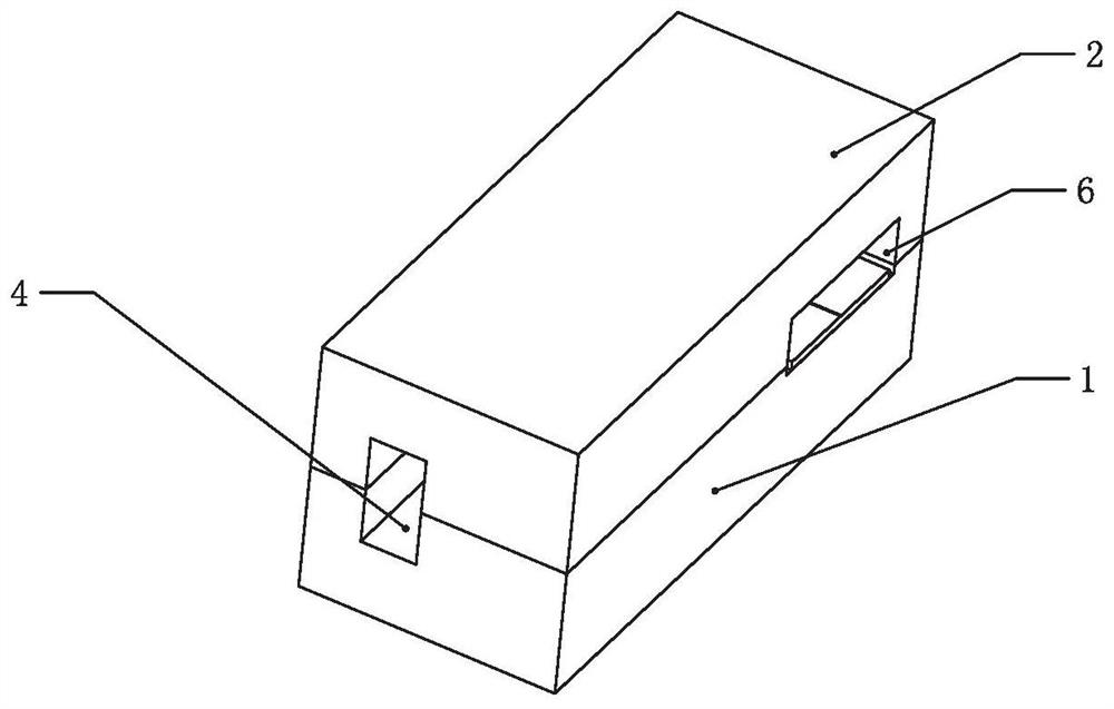
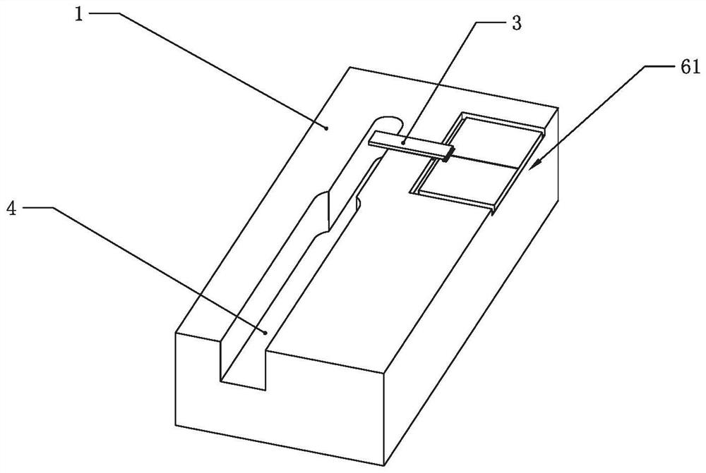
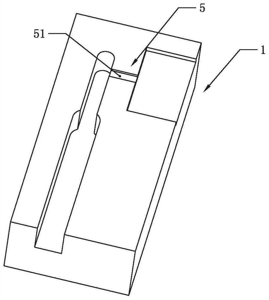
[0031] like Figure 1 to Figure 4 As shown, the present invention provides a transition structure for terahertz jumperless inverted coplanar waveguide monolithic circuit packaging, including a lower cavity 1, an upper cavity 2 and a coplanar waveguide circuit 3, and the upper cavity 2 is covered with the lower cavity A rectangular waveguide cavity 4, a coplanar waveguide circuit shielding cavity 5 and a monolithic circuit shielding cavity 6 are formed on the body 1 in sequence. In the planar waveguide circuit shielding cavity 5 , the coplanar waveguide circuit 3 is connected to the monolithic circuit 61 ; the electromagnetic signal enters from the rectangular waveguide cavity 4 , and is processed by the coplanar waveguide circuit 3 , and is output from the monolithic circuit shielding cavity 6 .

[0032] The coplanar waveguide circuit shieldin...


PUM


Abstract

The invention discloses a terahertz jumper-free inverted coplanar waveguide monolithic circuit package transition structure, which is characterized in that it includes a lower cavity, an upper cavity and a coplanar waveguide circuit, and the upper cavity is sealed on the lower cavity. The rectangular waveguide cavity, the coplanar waveguide circuit shielding cavity and the monolithic circuit shielding cavity connected in sequence, the monolithic circuit is installed in the monolithic circuit shielding cavity, the coplanar waveguide circuit is installed in the coplanar waveguide circuit shielding cavity, and the coplanar waveguide circuit Connected to a monolithic circuit; a terahertz jumperless inverted coplanar waveguide monolithic circuit packaging transition structure provided by the present invention can reduce the energy loss of the chip packaging structure in the terahertz frequency band, improve packaging performance, and reduce process complexity and cost, simple structure, convenient design and manufacture.

Description

technical field [0001] The invention belongs to the field of monolithic circuit packaging technology and terahertz device technology, and in particular relates to a transitional structure of a terahertz jumper-free inverted coplanar waveguide monolithic circuit packaging. Background technique [0002] Terahertz covers a wide spectrum range from 100GHz to 10THz, with a wavelength range of 3 mm to 30 microns, and has some characteristics of microwave and infrared. Its spectral range is wider than that of microwaves, the information capacity is increased, and it is suitable for high-speed and large-capacity communication; the signal-to-noise ratio of terahertz radiation is high, and it is suitable for high-quality imaging; its radiation energy is small, and it can penetrate ceramics, fabrics, plastics, and fats. and other materials, the attenuation is small. Terahertz monolithic circuits include terahertz amplifiers, frequency multipliers, mixers, signal transceiver systems, e...

Claims


Application Information

Patent Timeline
Patent Type & Authority Patents(China)
IPC IPC(8): H01P5/08
CPCH01P5/08
Inventor 张勇陈亚培徐锐敏郑权李骁孙岩
Owner UNIV OF ELECTRONICS SCI & TECH OF CHINA
Why Eureka
Try Eureka