High-voltage fast recovery diode structure

A technology for recovering diodes and diodes, which is applied in the direction of electrical components, circuits, semiconductor devices, etc., and can solve problems such as poor soft recovery performance and weak current shutdown capability, and achieve improved reverse recovery softness, good process compatibility, and improved The Effect of Area Efficiency and Chip Withstand Voltage Capability

Active Publication Date: 2017-11-10
BEIJING UNIV OF TECH
View PDF3 Cites 2 Cited by
  • Summary
  • Abstract
  • Description
  • Claims
  • Application Information

AI Technical Summary

Problems solved by technology

[0004] In order to overcome the defects of poor soft recovery performance and weak current turn-off ability of double-sided terminal diodes, the present invention combines double-sided terminal diodes with local p+ doped cathode region diodes to provide a high-voltage fast recovery diode structure

Method used


Image

  • High-voltage fast recovery diode structure
  • High-voltage fast recovery diode structure
  • High-voltage fast recovery diode structure

Examples


Embodiment 1

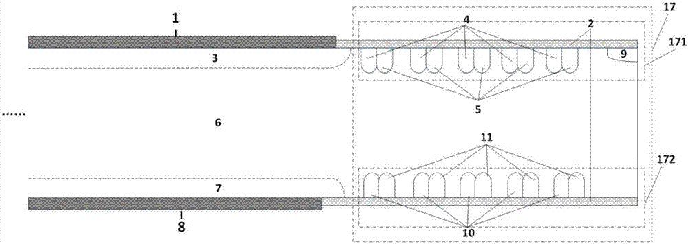
[0034] In this embodiment, the high-voltage fast recovery diode, such as figure 2 As shown, the back local p+ doping region 12 is on the surface of the cathode, and the doping dose is 1×10 15 ~1×10 18 cm -2 , the width is 1-10 μm, the thickness is 1-10 μm, and the arrangement pitch is 1-10 μm. The high-voltage fast recovery diode terminals are all double-sided terminals, including a front terminal area 171 and a rear terminal area 172, respectively surrounding the anode area and the cathode area. The front terminal region 171 is arranged on the anode side of the diode, and includes one of field plates, field limiting rings, semi-insulating thin film layers, and junction terminal extension structures with laterally variable doping, or two or more of them. Combination; the back termination region 172 is arranged on the cathode side of the diode, including one of a field plate, a field limiting ring, a semi-insulating thin film layer, and a junction termination extension stru...

Embodiment 2

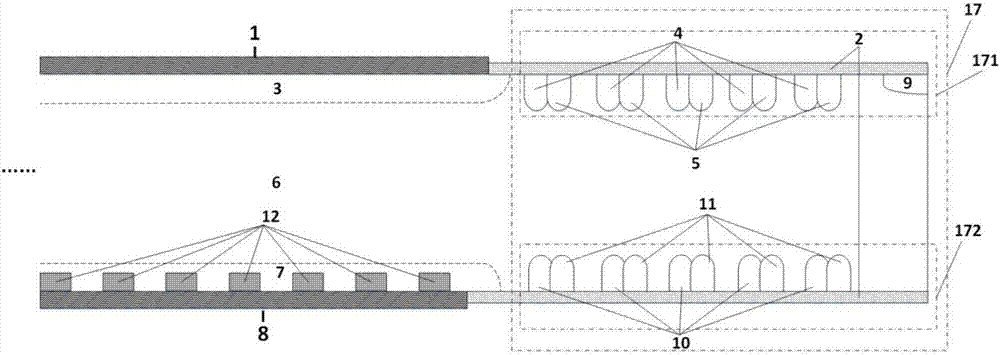
[0036] In this embodiment, the high-voltage fast recovery diode, such as image 3 As shown, the back local p+ doped region 12 is inside the cathode, and the doping dose is 1×10 15 ~1×10 18 cm -2 , the depth to the surface of the cathode region is 1-10 μm, the width is 1-10 μm, the thickness is 1-10 μm, and the arrangement pitch is 1-10 μm. The high-voltage fast recovery diode terminals are all double-sided terminals, including a front terminal area 171 and a rear terminal area 172, respectively surrounding the anode area and the cathode area. The front terminal region 171 is arranged on the anode side of the diode, and includes one of field plates, field limiting rings, semi-insulating thin film layers, and junction terminal extension structures with laterally variable doping, or two or more of them. Combination; the back termination region 172 is arranged on the cathode side of the diode, including one of a field plate, a field limiting ring, a semi-insulating thin film la...


PUM


Abstract

The invention provides a high-voltage fast recovery diode structure, and particularly relates to a double-sided terminal diode provided with a local p+ doping region negative electrode structure. The high-voltage fast recovery diode structure comprises an n- drift region, a positive electrode region, a local p+ doping negative electrode region and a double-sided terminal region, wherein the double-sided terminal structure comprises a front-surface terminal region and a back-surface terminal region, the front-surface terminal region and the back-surface terminal region are respectively encircled around the positive electrode region and the negative electrode region, so that the area efficiency of the terminal structure can be improved. The local p+ doping region is arranged on a surface of a back-surface negative electrode region or in the back-surface negative electrode region, different doping dosages, widths, depths and arrangement periods can be employed according to different application demands, holes can be injected in a reverse recovery tail period, electric field peak and current silkening at a negative electrode side can be prevented, and thus, the problem that a high punch-through effect brought by a double-sided terminal is not beneficial for improving the firmness of the high-voltage fast recovery diode structure and improving flexibility is solved.

Description

Technical field: [0001] The invention relates to the technical field of semiconductors, in particular to a high-voltage fast recovery diode structure. Background technique: [0002] The double-sided terminal structure has been proposed (Chinese invention patent application number: 201610685489.X), such as figure 1 As shown, the concentration of the substrate is required to be lower than the conventional situation, and the thickness of the silicon wafer is thin, in order to deplete the backside and make the backside terminal work. Although the double-sided terminal can improve the area efficiency of the terminal structure, this structure causes a strong punch-through of the electric field on the back side and increases the electric field on the cathode side, which will bring at least two hazards. 1. The remaining stored charge is quickly depleted during reverse recovery, resulting in current tripping and high voltage overshoot with very high di / dt, which may generate high el...

Claims


Application Information

Patent Timeline
Patent Type & Authority Applications(China)
IPC IPC(8): H01L29/861H01L29/06
CPCH01L29/0619H01L29/0684H01L29/861
Inventor 吴郁刘晨静李彭郭勇
Owner BEIJING UNIV OF TECH
Why Eureka
Try Eureka