LED integrated packaging structure and packaging method thereof

A technology that integrates packaging and packaging methods, applied in electrical components, electrical solid-state devices, circuits, etc., can solve the problems of low light efficiency and small output angle of COB packaging, and achieve the effect of increasing the output angle and improving light output efficiency.

Inactive Publication Date: 2017-11-14
SUZHOU INST OF NANO TECH & NANO BIONICS CHINESE ACEDEMY OF SCI
View PDF6 Cites 3 Cited by
  • Summary
  • Abstract
  • Description
  • Claims
  • Application Information

AI Technical Summary

Problems solved by technology

[0003] In order to solve the above problems, the LED COB structure and its packaging method proposed by the present invention can solve the problems of low light efficiency and small exit angle in COB packaging.

Method used


Image

  • LED integrated packaging structure and packaging method thereof
  • LED integrated packaging structure and packaging method thereof

Examples


Embodiment Construction

[0022] Hereinafter, embodiments of the present invention will be described in detail with reference to the accompanying drawings. The present invention may, however, be embodied in many different forms and should not be construed as limited to the specific embodiments set forth herein. Rather, these embodiments are provided to explain the principles of the invention and its practical application, to thereby enable others skilled in the art to understand the invention for various embodiments and with various modifications as are suited to the particular intended use.

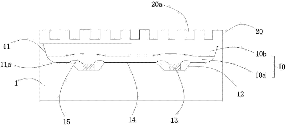
[0023] refer to figure 1 , This embodiment provides an LED COB structure, which includes a substrate 1, and the substrate 1 is a metal substrate. The upper surface of the substrate 1 is provided with a packaging glue groove 11 , and a bottom 11 a of the packaging glue groove 11 is provided with a die bonding groove array including a plurality of bowl-shaped die bonding grooves 12 , and the bottom of each die bon...


PUM


Abstract

The invention provides an LED integrated packaging structure, which comprises a substrate, a packaging adhesive groove formed in the upper surface of the substrate, and a microstructure layer arranged on the packaging adhesive groove, wherein a die boding groove array comprising a plurality of die bonding grooves are formed in the packaging adhesive groove, the bottom part of each die bonding groove is provided with an LED chip, a circuit board is further arranged in the packaging adhesive groove, an opening corresponding to the die boding groove array is formed in the circuit board, the LED chips are connected with the circuit board by means of lead wires, and the packaging adhesive groove is further filled with a packaging adhesive layer used for packaging the LED chips, the lead wires and the circuit board. According to the LED integrated packaging structure and a packaging method thereof provided by the invention, the microstructure layer covers the a fluorescent adhesive layer of the integrated packaging structure, and refractive indexes of a protective layer, the fluorescent layer and the microstructure layer are in a descending order, therefore the light emitting efficiency of the integral LED integrated packaging structure can be improved and the emergent angle thereof can be increased by adopting the design.

Description

technical field [0001] The invention relates to a semiconductor light-emitting device and a packaging method thereof, in particular to an LED integrated packaging structure and a packaging method thereof. Background technique [0002] Light Emitting Diode (LED) is a semiconductor component, which has the characteristics of energy saving, environmental protection, long life and small size, and is widely used in various fields such as indication, display, decoration, backlight, general lighting and urban night scenes. . In the LED device manufacturing process, LED packaging is the most important link in the manufacturing process, and this link directly affects the luminous efficiency of the LED device. At present, the most commonly used LED packaging is the integrated packaging (COB) technology. In COB technology, the LED light source is directly attached to the mirror metal substrate with high reflectivity. This technology eliminates the concept of brackets, and has no elect...

Claims


Application Information

Patent Timeline
Patent Type & Authority Applications(China)
IPC IPC(8): H01L33/52H01L33/58H01L33/00H01L25/075
CPCH01L33/52H01L25/0753H01L33/005H01L33/58
Inventor 王敏锐桑伟华王龙林露张宝顺
Owner SUZHOU INST OF NANO TECH & NANO BIONICS CHINESE ACEDEMY OF SCI
Why Eureka
Try Eureka