Display panel and manufacturing method thereof

A display panel and manufacturing method technology, applied in nonlinear optics, instruments, optics, etc., can solve the problems of serious signal delay, optimize panel performance, disadvantages, etc., achieve the effect of reducing impedance, reducing display delay, and improving display effect

Inactive Publication Date: 2017-11-17
TCL CHINA STAR OPTOELECTRONICS TECH CO LTD
View PDF9 Cites 13 Cited by
  • Summary
  • Abstract
  • Description
  • Claims
  • Application Information

AI Technical Summary

Problems solved by technology

The metal design with slits will have a much higher impedance than metals of the same width, an

Method used


Image

  • Display panel and manufacturing method thereof
  • Display panel and manufacturing method thereof
  • Display panel and manufacturing method thereof

Examples


Example Embodiment

[0014] The technical solutions in the embodiments of the present invention will be clearly and completely described below in conjunction with the accompanying drawings in the embodiments of the present invention. Obviously, the described embodiments are only a part of the embodiments of the present invention, rather than all the embodiments. Based on the embodiments of the present invention, all other embodiments obtained by those of ordinary skill in the art without creative work shall fall within the protection scope of the present invention.
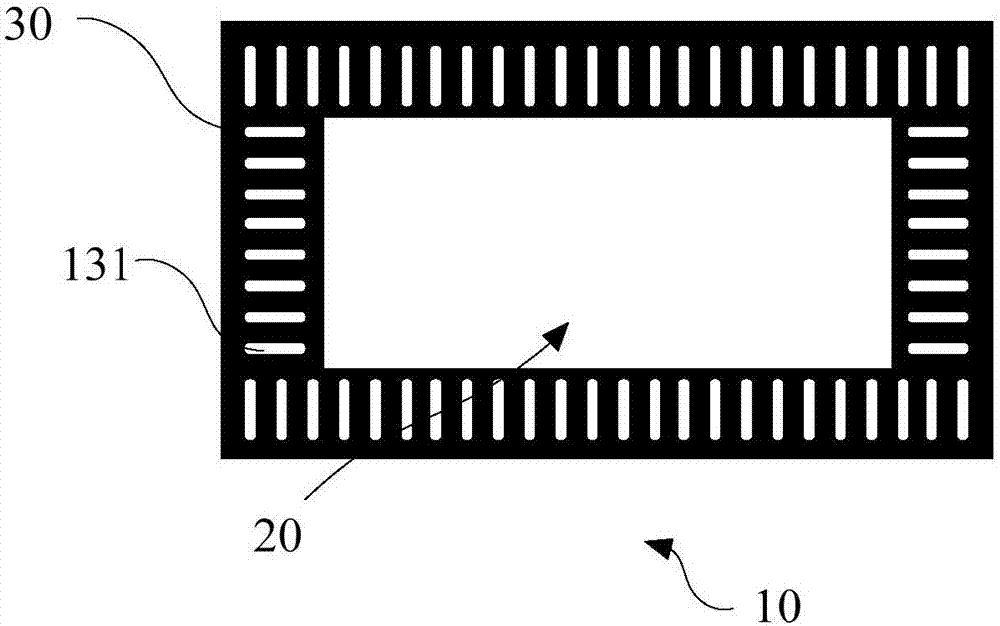
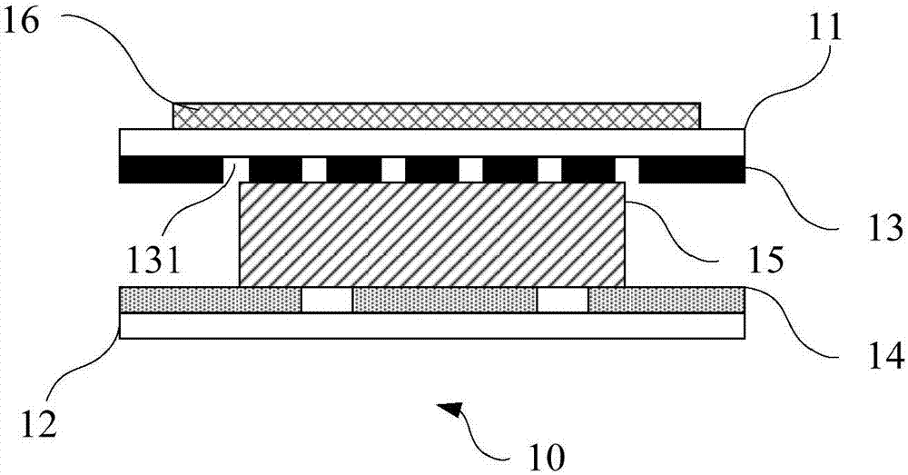
[0015] See figure 1 with figure 2 , figure 1 Is a schematic top view of the first embodiment of the display panel provided by the present invention, figure 2 It is a schematic partial cross-sectional view of the first embodiment of the display panel provided by the present invention. The display panel 10 includes a color filter substrate 11, a thin film transistor substrate 12, a light curing glue 15, and a light shielding layer 16. Am...


PUM


Abstract

The invention displays a display panel and a manufacturing method thereof. The display panel comprises a colored filtering substrate, a thin film transistor substrate, a light shading black matrix, a metal line, a light curing adhesive and a light shading layer, wherein the light shading black matrix is located in a non-display area of the colored filtering substrate, and seams are formed in the light shading black matrix; the metal line is located in a non-display area of the thin film transistor substrate; the light curing adhesive is located between the light shading black matrix and the metal line; the light shading layer is located on one side of the colored filtering substrate and correspond to the light shading black matrix. In this way, the frame glue curing of the display panel can be achieved, the signal delay problem of the display panel can be effectively alleviated, meanwhile, light rays can be effectively prevented from leaking out, and the display effect is improved.

Description

technical field [0001] The invention relates to the display field, in particular to a display panel and a manufacturing method thereof. Background technique [0002] Narrow bezel design is currently a common design for VA (Vertical Alignment, Vertical Alignment) liquid crystal displays. For this kind of design, it is generally realized by connecting different layers of metal on the bus through via holes, which requires the use of light-curing adhesives to bond The upper and lower substrates can be sealed. [0003] The curing light source is generally irradiated from a TFT (Thin Film Transistor, thin film transistor) substrate, and the photocurable adhesive is cured after the light is irradiated. Therefore, the metal traces under the light-curable adhesive are generally designed with slits, which is beneficial for the light to project through the TFT substrate and irradiate the light-curable adhesive to promote its curing. The metal design with slits will have a much higher...

Claims


Application Information

Patent Timeline
IPC IPC(8): G02F1/1339G02F1/1335G02F1/1333
CPCG02F1/1333G02F1/133512G02F1/1339
Inventor 赵丽王醉
Owner TCL CHINA STAR OPTOELECTRONICS TECH CO LTD
Why Eureka
Try Eureka