Ultraviolet detector array structure based on interdigital electrodes
A technology of ultraviolet detectors and interdigitated electrodes, which is applied in the field of optoelectronics, can solve problems such as substrate damage, and achieve the effects of low power consumption, fast response speed, and uniform film growth
- Summary
- Abstract
- Description
- Claims
- Application Information
AI Technical Summary
Problems solved by technology
Method used
Image

Examples
Embodiment 1
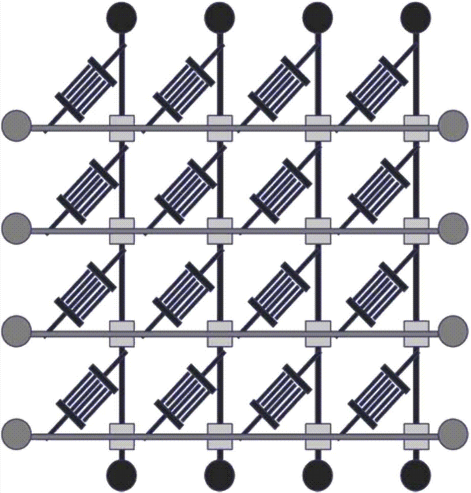
[0039] Taking a 4×4 detector array as an example, a standard semiconductor photolithography process is used, such as figure 1 As shown, if a high level is applied to a certain column conductor and a low level is applied to a certain row conductor, the interdigitated electrode element at the intersection of the row conductor and the column conductor will be in the working state due to the applied bias.
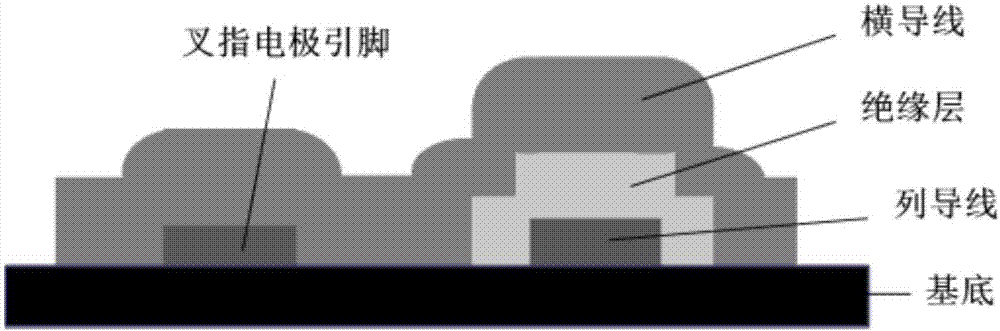
[0040] The cross-section of the structure along the row of wires is as follows figure 2 As shown, it includes a base layer, a lower electrode layer, an insulating layer and an upper electrode layer.
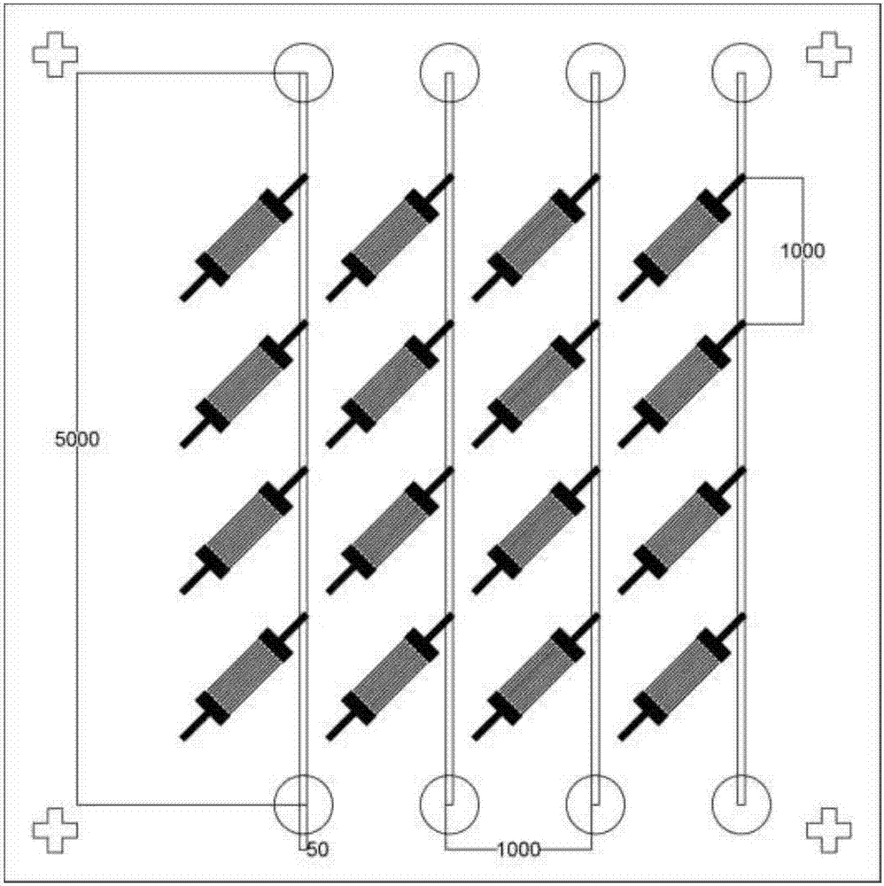
[0041] Firstly, realize the array of column wires and interdigitated electrodes, and the upper electrode mask such as image 3 As shown, the distance between the centers of two adjacent interdigitated electrodes is 1000 μm, the finger width is 10 μm, and they are arranged at an angle of 45 degrees to the column conductors. The column conductors are 5000 μm long and 50 μm wide, e...
PUM
 Abstract
Description
Claims
Application Information