A kind of film layer structure, display device and preparation method of film layer structure

A technology of film layer structure and laminated structure, which is applied in semiconductor/solid-state device manufacturing, organic semiconductor devices, semiconductor devices, etc., can solve problems such as affecting the life of OLED devices and being prone to cracking.

Active Publication Date: 2020-07-28
BOE TECH GRP CO LTD +1
View PDF6 Cites 0 Cited by
  • Summary
  • Abstract
  • Description
  • Claims
  • Application Information

AI Technical Summary

Problems solved by technology

[0005] The present invention provides a film layer structure, a display device and a method for preparing the film layer structure, so as to solve the existing problem that the film layer deposited on the organic film layer is prone to breakage at the corner position, which affects the life of the OLED device

Method used


Image

  • A kind of film layer structure, display device and preparation method of film layer structure
  • A kind of film layer structure, display device and preparation method of film layer structure
  • A kind of film layer structure, display device and preparation method of film layer structure

Examples


Embodiment 1

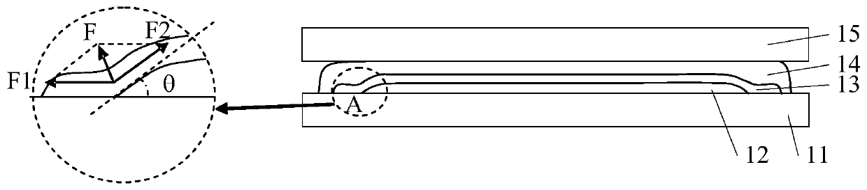
[0036] refer to figure 1 , showing one of the schematic diagrams of the film layer structure in the embodiment of the present invention.

[0037] An embodiment of the present invention provides a film layer structure, which is applied to an electroluminescent display panel. The electroluminescent display panel includes a substrate, and a first organic film layer 12 is disposed on the substrate 11; the first organic film Layer 12 is an organic film layer whose outer edge is closest to the edge of the substrate 11 in the film layer structure, and the climbing angle between the first organic film layer 12 and the substrate 11 is smaller than the breakable angle.

[0038] In the embodiment of the present invention, the substrate 11 may be a rigid substrate or a flexible substrate.

[0039] like figure 1 As shown, the schematic diagram on the left is a partial enlarged view of region A (the position of the dotted circle) in the film layer structure, the climbing angle between the...

Embodiment 2

[0064] An embodiment of the present invention also provides a display device, which includes the above-mentioned film layer structure, and the film layer structure is applied to an electroluminescent display panel, and the electroluminescent display panel includes a substrate, and the substrate is provided with the first organic film layer;

[0065] The first organic film layer is the organic film layer whose outer edge of the film layer is closest to the edge of the substrate in the film layer structure, and the climbing angle between the first organic film layer and the substrate is smaller than the breakable angle

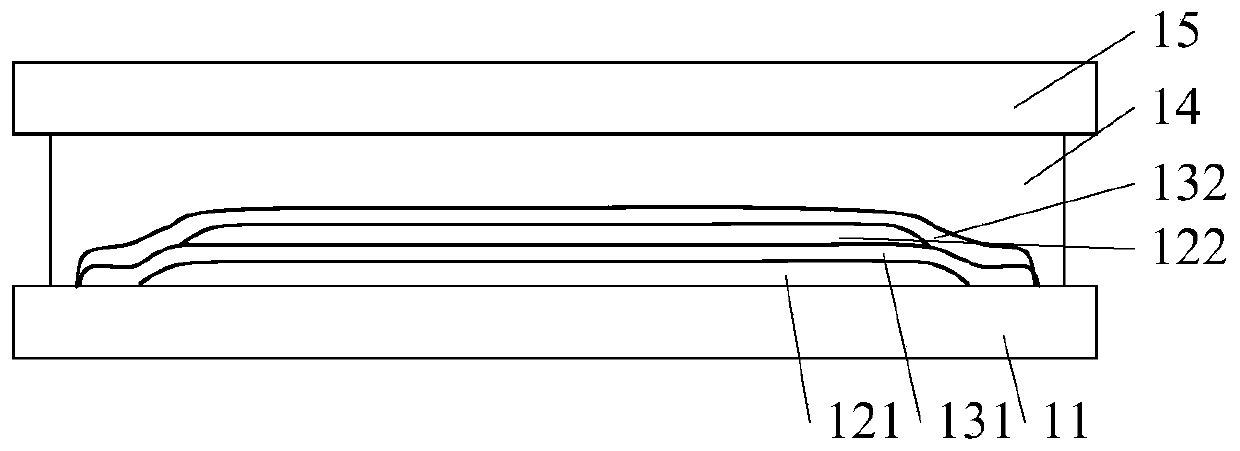
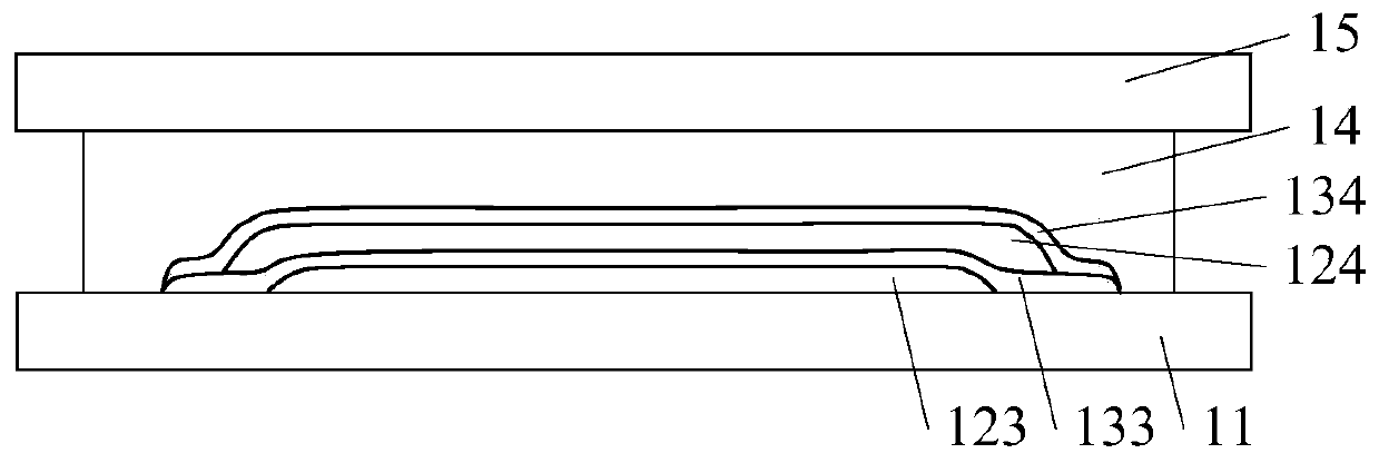
[0066] Wherein, the breakable angle is 35°; the first organic film layer is the organic film layer in the backplane structure or the organic film layer in the packaging structure; the first organic film layer is also provided with a first inorganic film layer.

[0067] In one embodiment of the present invention, the first organic film layer is an organic film l...

Embodiment 3

[0073] refer to Figure 4 , shows a flow chart of a method for preparing a film layer structure in an embodiment of the present invention.

[0074] Step 401, forming a first organic film layer on a substrate.

[0075] In the embodiment of the present invention, firstly, the first organic film layer is formed on the substrate. Since the types of the first organic film layer are different, their preparation methods are also different.

[0076] Wherein, the first organic film layer is the organic film layer whose outer edge of the film layer is closest to the edge of the substrate in the film layer structure, and the climbing angle between the first organic film layer and the substrate is smaller than angle.

[0077] refer to figure 2 , when the first organic film layer 121 is an organic film layer in the backplane structure, the first organic film layer 121 is formed by exposure and development processes, by adjusting the exposure intensity, exposure time, developer concentr...


PUM


Abstract

The invention provides a film layer structure, a display device and a preparation method of the film layer structure, and relates to the field of display technology. In the present invention, a first organic film layer is provided on the substrate, and the first organic film layer is an organic film layer whose outer edge of the film layer is closest to the edge of the substrate in the film layer structure, and the first organic film layer The climbing angle of the layer to the substrate is less than the susceptibility angle. By controlling the climbing angle between the first organic film layer and the substrate to be smaller than the breakable angle, the climbing slope angle of the film layer subsequently formed on the first organic film layer is reduced, thereby reducing the angle of the film layer formed subsequently at the corner position Due to the resultant force generated by the stress in two directions, the subsequently formed film layers are prevented from cracking, and the service life of the OLED device is improved.

Description

technical field [0001] The invention relates to the field of display technology, in particular to a film layer structure, a display device and a preparation method of the film layer structure. Background technique [0002] OLED (Organic Light Emitting Diode, organic electroluminescent device) has many advantages such as active light emission, high brightness, high contrast, ultra-thin, low power consumption, flexibility and wide operating temperature range, and has become a very competitive and developing Prospects for next-generation display technologies. [0003] In an OLED device, the thickness of the organic film layer formed on the substrate is at the micron level. Due to the limitation of the formation process and material of the organic film layer, the climbing angle between the upper surface of the organic film layer and the substrate is relatively large. [0004] When depositing other film layers on the organic film layer, due to the relatively large climbing angle...

Claims


Application Information

Patent Timeline
Patent Type & Authority Patents(China)
IPC IPC(8): H01L51/52H01L51/56
CPCH10K50/844H10K71/00H10K59/124H10K59/122H10K50/8445H10K50/8426H10K77/111H10K2102/311
Inventor 王玉林施槐庭宋丽芳彭锐
Owner BOE TECH GRP CO LTD
Why Eureka
Try Eureka