Pulse receiving circuit
A pulse receiving and circuit technology, applied in logic circuits, pulse technology, and logic circuits using optoelectronic devices, etc., can solve problems such as inconsistent signal strength, difference in received current, poor circuit stability and reliability, etc. The effect of less components and low cost
- Summary
- Abstract
- Description
- Claims
- Application Information
AI Technical Summary
Problems solved by technology
Method used
Image
Examples
Embodiment 1
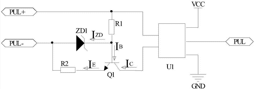
[0030] Such as figure 1 As shown, a pulse receiving circuit includes: a resistor R1, a resistor R2, a voltage regulator tube ZD1, an NPN transistor Q1 and a photocoupler U1.
[0031] One end of the resistor R1 is respectively connected to the PUL+ terminal of the pulse signal source and the first input port of the photocoupler U1, and the other end of the resistor R1 is respectively connected to the base of the NPN transistor Q1 and the cathode of the voltage regulator ZD1; one end of the resistor R2 is connected to The emitter of the NPN transistor Q1 and the other end of the resistor R2 are respectively connected to the PUL- terminal of the pulse signal source and the anode of the voltage regulator ZD1; the collector of the NPN transistor Q1 is connected to the second input port of the photocoupler U1.
[0032]The working principle of the circuit is as follows: when the high-frequency pulse signal PUL+ is at a high level (relative to PUL-), the current flows through the base...
Embodiment 2
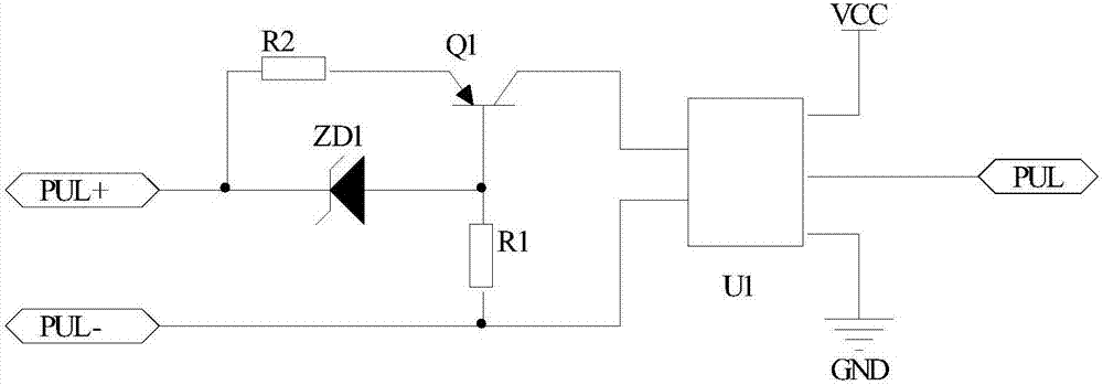
[0036] Such as figure 2 As shown, a pulse receiving circuit includes: a resistor R1, a resistor R2, a voltage regulator tube ZD1, a PNP transistor Q1 and a photocoupler U1.
[0037] One end of the resistor R1 is respectively connected to the PUL- end of the pulse signal source and the first input port of the photocoupler U1, and the other end of the resistor R1 is respectively connected to the base of the PNP transistor Q1 and the anode of the regulator tube ZD1; one end of the resistor R2 Connect the emitter of the PNP transistor Q1, the other end of the resistor R2 is respectively connected to the PUL+ terminal of the pulse signal source and the cathode of the voltage regulator ZD1; the collector of the NPN transistor Q1 is connected to the second input port of the photocoupler U1.
[0038] This circuit is a high-frequency pulse receiving circuit with high reliability and wide voltage range, which meets various working occasions of servo drives.
Embodiment 3
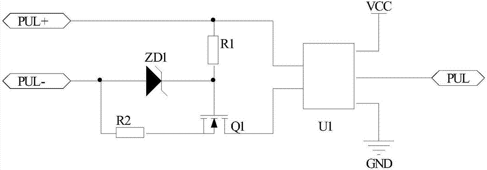
[0040] Such as image 3 As shown, a pulse receiving circuit includes: a resistor R1, a resistor R2, a voltage regulator tube ZD1, an N-channel MOS transistor Q1 and a photocoupler U1.
[0041] One end of the resistor R1 is respectively connected to the PUL+ terminal of the pulse signal source and the first input port of the photocoupler U1, and the other end of the resistor R1 is respectively connected to the gate of the N-channel MOS transistor Q1 and the cathode of the voltage regulator tube ZD1; the resistor R2 One end is connected to the source of the N-channel MOS transistor Q1, and the other end of the resistor R2 is connected to the PUL- terminal of the pulse signal source and the anode of the voltage regulator transistor ZD1 respectively; the drain of the N-channel MOS transistor Q1 is connected to the first terminal of the photocoupler U1 Two input ports.
[0042] This circuit is a high-frequency pulse receiving circuit with high reliability and wide voltage range, w...
PUM
 Abstract
Description
Claims
Application Information


