Supercharge Your Innovation With Domain-Expert AI Agents!

Cavity cleaning method for reducing lower electrode damage

A technology of electrodes and chambers, which is applied in the field of chamber cleaning to reduce the damage of the lower electrodes, can solve the problems of occupying equipment transmission resources, reducing production efficiency, increasing wafer consumption, etc., so as to prolong the service life, avoid damage to the lower electrodes, and save energy. Effect of Wafer Consumption

Inactive Publication Date: 2017-11-24
鲁汶仪器有限公司(比利时)
View PDF5 Cites 1 Cited by
  • Summary
  • Abstract
  • Description
  • Claims
  • Application Information

AI Technical Summary

Problems solved by technology

However, due to the need for additional companion pieces, the wafer consumption is increased, and at the same time, the transmission block needs to be interspersed during the production process, which occupies equipment transmission resources and reduces production efficiency
[0006] To sum up, the current plasma cleaning process cannot solve the problems of base (bottom electrode) life, wafer consumption and equipment transmission efficiency.

Method used


Image

  • Cavity cleaning method for reducing lower electrode damage
  • Cavity cleaning method for reducing lower electrode damage
  • Cavity cleaning method for reducing lower electrode damage

Examples


Embodiment 1

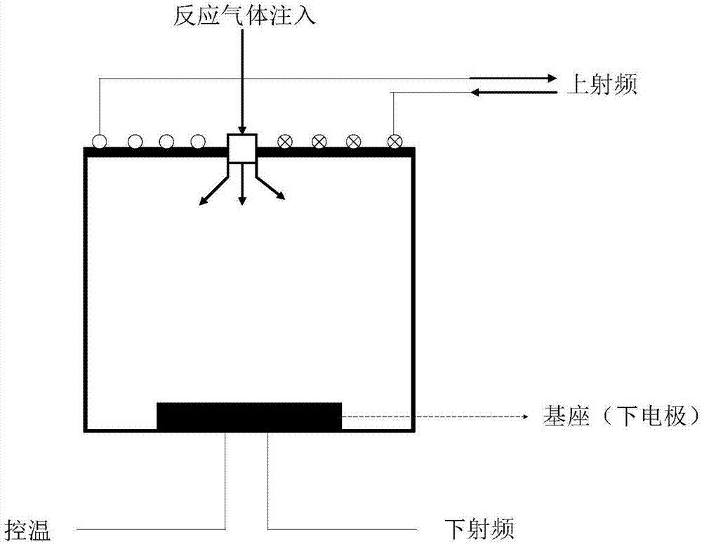
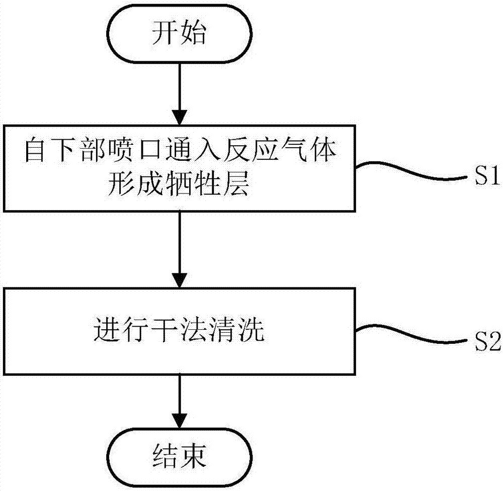
[0032] The inductively coupled plasma etching machine is used to etch silicon deeply, and the process gas for etching silicon grooves is the well-known SF 6 and C 4 f 8 , during the etching process, the C produced by physical bombardment of Si and photoresist will be deposited on the wall of the ICP etching chamber. x h yWait. Chamber cleaning is performed between each wafer to reduce damage to the bottom electrode.

[0033] In the sacrificial layer forming step S1, the power of the upper electrode is turned off, the power of the lower electrode is set between 50W and 500W, the pressure of the chamber is set between 3mT and 100mT, and the C 4 f 8 Gas, the gas flow rate is 20sccm~200sccm, the feeding time is 3s~20s, and 10nm~100nm of C is deposited on the surface of the lower electrode. x f y as a sacrificial layer. The reaction gas is introduced from the lower nozzle and the power of the lower electrode is started, so that C x f y concentrated deposition on the surfa...

Embodiment 2

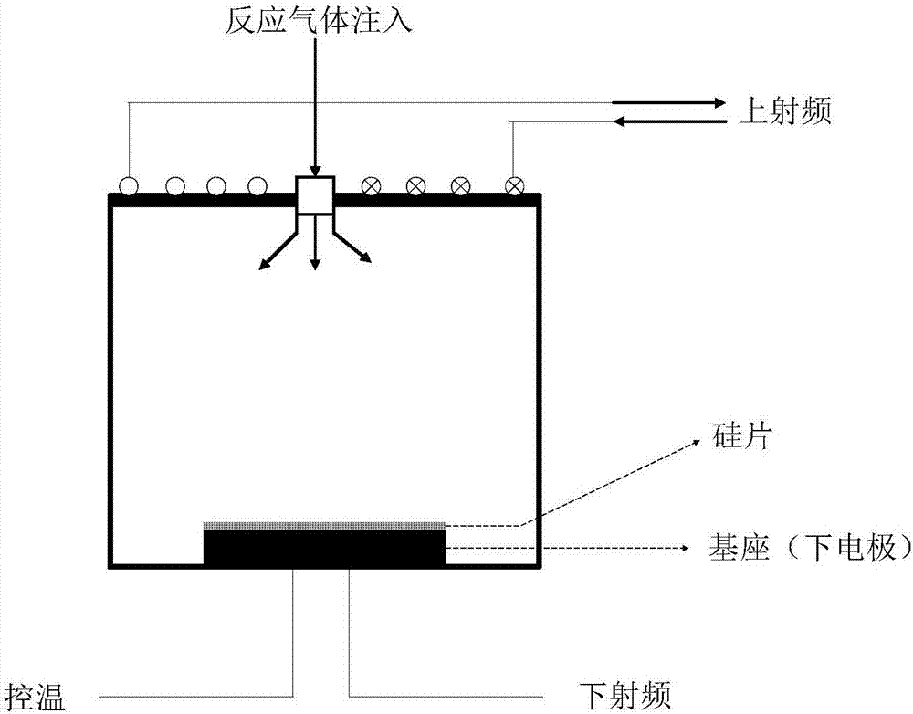
[0036] Silicon is etched using an inductively coupled plasma etching machine, and the process gas for etching silicon is the well-known Cl 2 / HBr / O 2 , during the etching process, the Si produced by physical bombardment of Si and photoresist will be deposited on the wall of the etching chamber, C x h y And SiBr, which is not volatile under plasma reaction 4 , SiBr x o y , SiCl x o y Wait. Chamber cleaning is performed between each wafer to reduce damage to the bottom electrode.

[0037] In the sacrificial layer forming step S1, the power of the upper electrode is turned off, the power of the lower electrode is set between 100W and 500W, the chamber pressure is set between 3mT and 100mT, and SiH is injected through the lower nozzle 4 gas and NH 3 gas, where SiH 4 The flow rate is 20sccm~200sccm, NH 3 The feed flow rate is 20sccm-200sccm, the feed time is 3s-20s, and 30-100nm of SiN is deposited on the surface of the lower electrode as a sacrificial layer. The reacti...


PUM


Abstract

The invention discloses a cavity cleaning method for reducing lower electrode damage. The method comprises the following steps of forming a sacrificial layer for protecting a lower electrode, importing reaction gas through a lower nozzle near to the lower electrode, carrying out thin film deposition on the surface of the lower electrode, thereby forming the sacrificial layer for protecting the surface of the lower electrode; and carrying out dry cleaning, importing the reaction gas through an upper nozzle of a cavity and carrying out plasma cleaning on the cavity. According to the method, through introduction of the thin film deposition step, the lower electrode damage resulting from directly exposing the lower electrode in a plasma environment is avoided, the service life of the lower electrode is prolonged, moreover, the wafer consumption is reduced, the working efficiency of a device is improved, and the solutions of the problems in two aspects: the service life of the lower electrode, and the wafer consumption and the transmission efficiency of the device are taken into consideration effectively. Through change of a gas inflow mode, the controllability of the thin film deposition is effectively improved, the thin film is deposited on the surface of the lower electrode as much as possible, the working efficiency of the device is further improved, and the raw material cost is reduced.

Description

technical field [0001] The invention relates to the technical field of integrated circuits, in particular to a cavity cleaning method for reducing damage to lower electrodes. Background technique [0002] In the semiconductor process, it is often necessary to perform a plasma cleaning process between batches of wafers (or between single wafers) to maintain a stable chamber environment and improve process repeatability, stability, and yield. For example, in the plasma etching process, due to the bombardment of the plasma on the surface of the silicon wafer and the reaction between the process gas and the surface material of the wafer, some process by-products, such as polymers, are often attached to the inner wall surface of the chamber, while the lower electrode is etched. It is blocked by etching silicon wafers, so there is no etching by-products attached to the surface. In order to remove the process by-products produced by the etching process, the currently applied metho...

Claims


Application Information

Patent Timeline
Patent Type & Authority Applications(China)
IPC IPC(8): H01J37/32
CPCH01J37/32862
Inventor 康斯坦丁·莫吉利尼科夫
Owner 鲁汶仪器有限公司(比利时)
Features
  • R&D
  • Intellectual Property
  • Life Sciences
  • Materials
  • Tech Scout
  • Unparalleled Data Quality
  • Higher Quality Content
  • 60% Fewer Hallucinations
Learn More