

Method for manufacturing chip-mounting substrate, and chip-mounting substrate
A chip mounting and substrate technology, which is applied in semiconductor/solid-state device manufacturing, semiconductor/solid-state device components, semiconductor devices, etc., can solve the problems of difficult to manufacture masks, reduce the precision of planar masks, and separate masks, etc., and achieve improved The effect of reducing bonding force and manufacturing cost
- Summary
- Abstract
- Description
- Claims
- Application Information
AI Technical Summary
Problems solved by technology
Method used
Image

Examples
Embodiment Construction
[0044] Embodiments of the present invention will now be described in detail with reference to the accompanying drawings.
[0045] For the same structure of the present invention as the prior art, reference is made to the prior art. A detailed description thereof will be omitted.
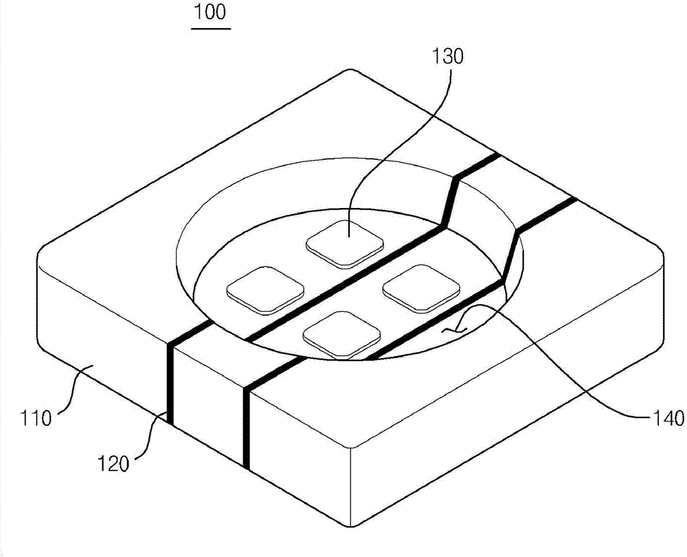
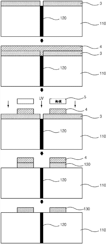
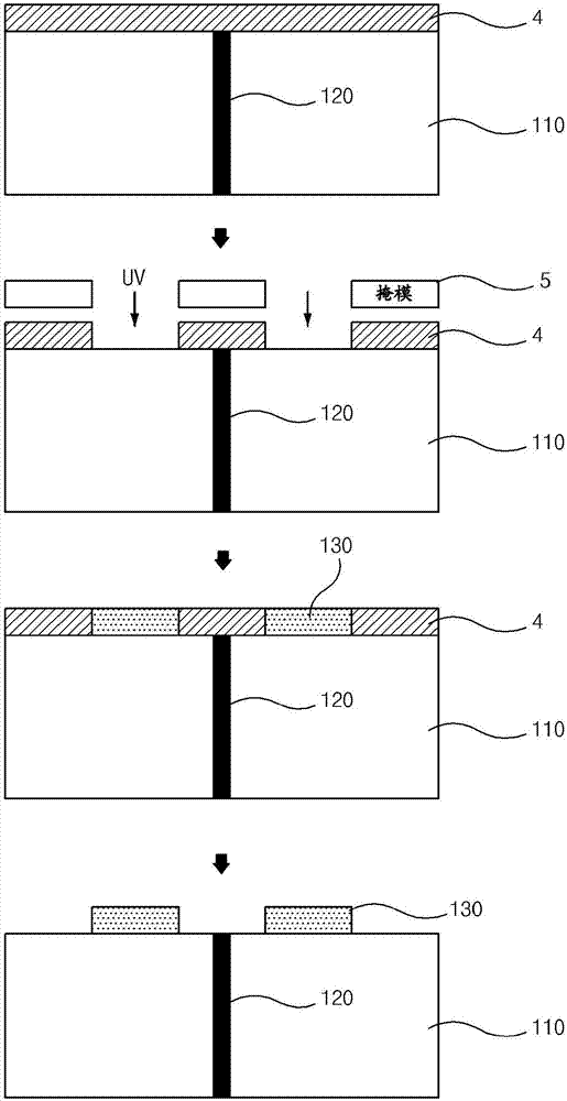
[0046] refer to Figure 4 , according to the manufacturing method of the chip mounting substrate of the embodiment of the present invention, comprise: the pre-coating step that forms pre-coating layer 60 on the metal substrate 10 that is divided into two conductive parts by insulating part 20; ) an etching step of etching at least a part of the precoat layer 60 to form a pattern 50; and a step of forming the metal layer 30 on the metal substrate 10, wherein the pattern 50 is provided on at least one of the two conductive portions divided by the insulating portion 20 , and the metal layer 30 is formed in the pattern 50 .
[0047] The method of this embodiment may further include a cavity forming st...
PUM
 Abstract
Description
Claims
Application Information