Method for directly bonding silicon slice with sapphire slice
A direct bonding and sapphire technology, which is applied in welding equipment, pattern surface photolithography, precision positioning equipment, etc., can solve problems such as low bonding quality, lower qualified rate of bonded products, and irregular chipping of silicon wafers, etc. problem, achieve the effect of improving bonding quality and preventing random fragmentation
- Summary
- Abstract
- Description
- Claims
- Application Information
AI Technical Summary
Problems solved by technology
Method used
Image

Examples
Embodiment 1
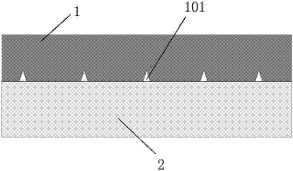
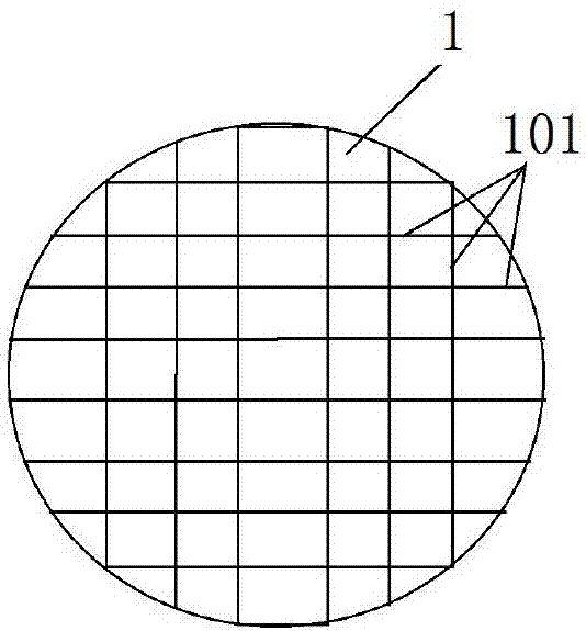
[0019] A method for direct bonding of a silicon wafer 1 and a sapphire wafer 2, comprising the following steps:
[0020] 1) prepare the polished silicon wafer 1 and the polished sapphire wafer 2, etch the stress relief groove 101 on one or both sides of the silicon wafer 1, and the stress relief groove 101 includes at least one first groove body and at least one A second tank, any one of the first tanks intersects any one of the second tanks;
[0021] 2) performing plasma activation treatment on the surface having the stress relief groove 101 on the silicon wafer 1, and performing plasma activation treatment on the single side of the sapphire wafer 2;
[0022] 3) Pre-bonding the surface of the silicon wafer 1 that has undergone the plasma activation treatment and the surface of the sapphire wafer 2 that has undergone the plasma activation treatment;
[0023] 4) Annealing the pre-bonded silicon wafer 1 and sapphire wafer 2 to completely bond the silicon wafer 1 and the sapphir...
Embodiment 2
[0025] A method for direct bonding of a silicon wafer 1 and a sapphire wafer 2, comprising the following steps:
[0026] 1) prepare the polished silicon wafer 1 and the polished sapphire wafer 2, etch the stress relief groove 101 on one or both sides of the silicon wafer 1, and the stress relief groove 101 includes at least one first groove body and at least one A second tank, any one of the first tanks intersects any one of the second tanks;
[0027] 2) performing plasma activation treatment on the surface having the stress relief groove 101 on the silicon wafer 1, and performing plasma activation treatment on the single side of the sapphire wafer 2;
[0028] 3) Pre-bonding the surface of the silicon wafer 1 that has undergone the plasma activation treatment and the surface of the sapphire wafer 2 that has undergone the plasma activation treatment;
[0029] 4) Annealing the pre-bonded silicon wafer 1 and sapphire wafer 2 to completely bond the silicon wafer 1 and the sapphir...
Embodiment 3
[0031] A method for direct bonding of a silicon wafer 1 and a sapphire wafer 2, comprising the following steps:
[0032] 1) prepare the polished silicon wafer 1 and the polished sapphire wafer 2, etch the stress relief groove 101 on one or both sides of the silicon wafer 1, and the stress relief groove 101 includes at least one first groove body and at least one A second tank, any one of the first tanks intersects any one of the second tanks;
[0033] 2) performing plasma activation treatment on the surface having the stress relief groove 101 on the silicon wafer 1, and performing plasma activation treatment on the single side of the sapphire wafer 2;
[0034] 3) Pre-bonding the surface of the silicon wafer 1 that has undergone the plasma activation treatment and the surface of the sapphire wafer 2 that has undergone the plasma activation treatment;
[0035] 4) Annealing the pre-bonded silicon wafer 1 and sapphire wafer 2 to completely bond the silicon wafer 1 and sapphire wa...
PUM
 Abstract
Description
Claims
Application Information