Bonding structure and formation method thereof

A bonding structure and bonding technology, applied in the manufacture of electrical components, electrical solid devices, semiconductor/solid devices, etc., can solve the problems of peeling, easy bubbles, fragments, etc., and meet the requirements of reducing wafer alignment and improving Bonding quality and the effect of improving product yield

Active Publication Date: 2019-06-07
YANGTZE MEMORY TECH CO LTD
View PDF5 Cites 2 Cited by
  • Summary
  • Abstract
  • Description
  • Claims
  • Application Information

AI Technical Summary

Problems solved by technology

[0004] The hybrid bonding method requires strict alignment of the two wafers. Once there is a misalignment, the connection will fail and the yield will decrease.
Moreover, since the memory array wafer has a complex thin-film stack structure
During the bonding process of CMOS circuit wafers and storage array wafers, problems such as bubbles, peeling and even fragments are prone to occur. There are extremely high requirements for the quality of the contact interface of the wafers. The difference in deformation and stress between the two sides can easily lead to misalignment problems.

Method used


Image

  • Bonding structure and formation method thereof
  • Bonding structure and formation method thereof
  • Bonding structure and formation method thereof

Examples


Embodiment Construction

[0028] The specific implementation of the bonding structure provided by the present invention and its forming method will be described in detail below in conjunction with the accompanying drawings.

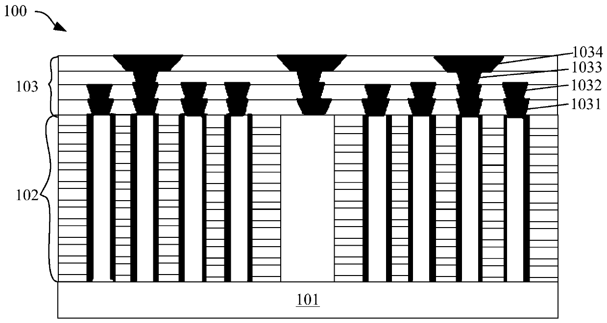
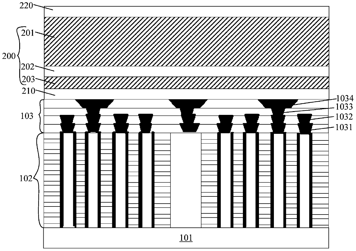
[0029] Please refer to Figure 1 to Figure 8 , is a structural schematic diagram of the formation process of the bonding structure according to a specific embodiment of the present invention.

[0030] Please refer to figure 1 , providing a first substrate 100, an electrical contact portion is formed in the first substrate 100, the first substrate has a first surface and a second surface opposite to each other, and the surface of the electrical contact portion is in contact with the first substrate of the first substrate. One surface is flush.

[0031] The first substrate 100 may be a semiconductor substrate, and a dielectric layer may be formed on the semiconductor substrate, as well as semiconductor devices and interconnection structures formed in the dielectric layer.

[003...


PUM


Abstract

The present invention relates to a bonding structure and a formation method thereof. The formation method of the bonding structure comprises the steps of: providing a first substrate, wherein an electric contact portion is formed in the first substrate, the first substrate has a first surface and a second surface which are opposite, and the surface of the electric contact portion is leveled with the first surface of the first substrate; providing a second substrate, and forming a bonding dielectric layer at the surface of one side of the second substrate; bonding the second substrate with thefirst surface of the first substrate through the bonding dielectric layer; and forming a semiconductor device at the surface of the other side of the second substrate. The bonding quality of the bonding structure is improved.

Description

technical field [0001] The invention relates to the technical field of semiconductors, in particular to a bonding structure and a forming method thereof. Background technique [0002] In recent years, the development of flash memory (Flash Memory) is particularly rapid. The main feature of flash memory is that it can keep stored information for a long time without power on, and has the advantages of high integration, fast access speed, easy erasing and rewriting, etc. Has been widely used. In order to further increase the bit density (Bit Density) of the flash memory while reducing the bit cost (Bit Cost), three-dimensional flash memory (3D NAND) technology has been developed rapidly. [0003] In the 3D NAND flash memory structure, it includes a storage array structure and a CMOS circuit structure above the storage array structure. The storage array junction and the CMOS circuit structure are usually formed on two different wafers respectively, and then through hybrid bond...

Claims


Application Information

Patent Timeline
IPC IPC(8): H01L21/768H01L21/50H01L23/538H01L23/00H01L25/00H01L25/18H01L27/11548H01L27/11551H01L27/11575H01L27/11578
Inventor 范鲁明刘毅华刘峻
Owner YANGTZE MEMORY TECH CO LTD
Why Eureka
Try Eureka