Preparation method and application of Ag surface plasmon-containing silicon-based LED

A surface plasmon, silicon-based technology, applied in the direction of electrical components, circuits, semiconductor devices, etc., can solve the problems of small amount of information, difficult integration, slow electron transmission speed, etc., to improve the intensity of electroluminescence, increase The Effect of Compounding Chances

Inactive Publication Date: 2017-12-12
GUIZHOU MINZU UNIV
View PDF0 Cites 3 Cited by
  • Summary
  • Abstract
  • Description
  • Claims
  • Application Information

AI Technical Summary

Problems solved by technology

[0002] Silicon is one of the most important semiconductor materials. It is abundant on the earth and has good mechanical and thermal properties. It rarely exists in the form of simple substances, mainly in the form of complex silicates or silicon dioxide, and silicon dioxide Not only is the insulation performance good, but it is also a very good diffusion barrier material, so silicon is the cornerstone of moder...

Method used


Image

  • Preparation method and application of Ag surface plasmon-containing silicon-based LED
  • Preparation method and application of Ag surface plasmon-containing silicon-based LED
  • Preparation method and application of Ag surface plasmon-containing silicon-based LED

Examples


Embodiment 1

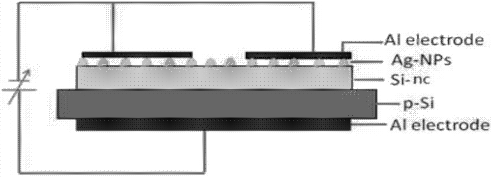
[0028] A method for preparing a silicon-based LED containing Ag surface plasmons, comprising the following steps:

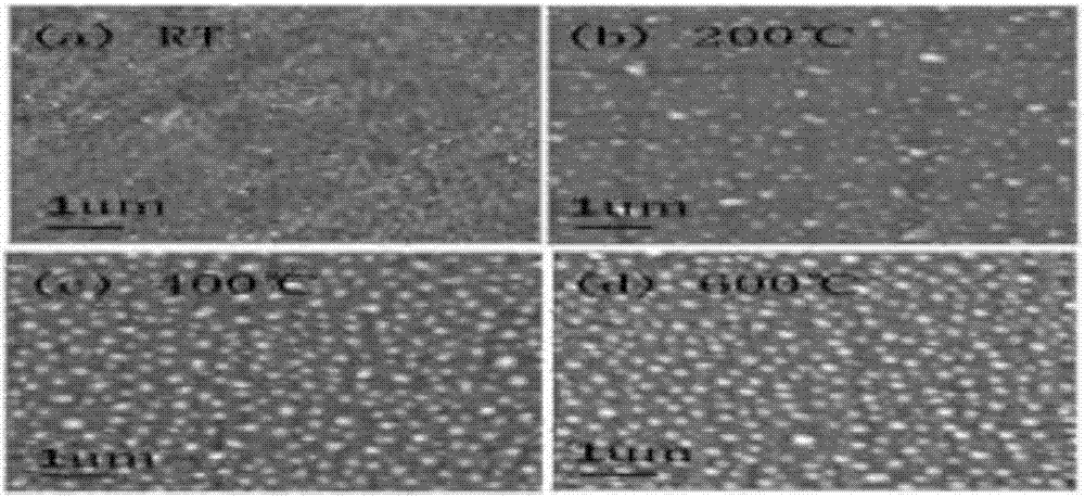
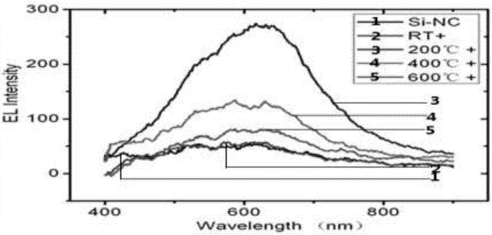
[0029] (1) Soaking: put the silicon nanocrystalline film into the AgNO 3 solution, after ultrasonic treatment for 30min, take it out and dry it with nitrogen gas.

[0030] (2) Primary annealing: perform thermal annealing in a high-temperature annealing furnace, the annealing temperature is 200° C., and the annealing time is 30 minutes to obtain a Si-nc film containing Ag nanoparticles;

[0031] (3) Secondary annealing: evaporating 2 μm of Al on the back side of the film described in step (2) as a positive electrode, performing thermal annealing in a high-temperature annealing furnace, the annealing temperature is 480 ° C, and the annealing time is 10 min;

[0032] (4) Three times of annealing; after step (3), vapor-deposit a 700nm Al ring on the front side of the Si-nc film as a negative electrode, and perform thermal annealing in a high-temperature annealing fu...

Embodiment 2

[0040] A method for preparing a silicon-based LED containing Ag surface plasmons, comprising the following steps:

[0041] (1) Soaking: put silicon nanocrystals into AgNO 3 solution, after ultrasonic treatment for 30min, take it out and dry it with nitrogen gas.

[0042] (2) Primary annealing: perform thermal annealing in a high-temperature annealing furnace, the annealing temperature is 400° C., and the annealing time is 30 minutes to obtain a Si-nc film containing Ag nanoparticles;

[0043] (3) Secondary annealing: evaporating 2 μm of Al on the back side of the film described in step (2) as a positive electrode, performing thermal annealing in a high-temperature annealing furnace, the annealing temperature is 480 ° C, and the annealing time is 10 min;

[0044] (4) Three times of annealing; after step (3), vapor-deposit an 800nm ​​Al ring on the front side of the Si-nc film as a negative electrode, and perform thermal annealing in a high-temperature annealing furnace with an...

Embodiment 3

[0052] A method for preparing a silicon-based LED containing Ag surface plasmons, comprising the following steps:

[0053] (1) Soaking: put the silicon nanocrystalline film into the AgNO 3 solution, after ultrasonic treatment for 30min, take it out and dry it with nitrogen gas.

[0054] (2) Primary annealing: perform thermal annealing in a high-temperature annealing furnace, the annealing temperature is 600° C., and the annealing time is 30 minutes to obtain a Si-nc film containing Ag nanoparticles;

[0055] (3) Secondary annealing: evaporating 2 μm of Al on the back side of the film described in step (2) as a positive electrode, performing thermal annealing in a high-temperature annealing furnace, the annealing temperature is 480 ° C, and the annealing time is 10 min;

[0056] (4) Three times of annealing; after step (3), a 900nm Al ring is vapor-deposited on the front side of the Si-nc film as a negative electrode, and thermal annealing is performed in a high-temperature an...


PUM

PropertyMeasurementUnit
Sizeaaaaaaaaaa
Resistivityaaaaaaaaaa

Abstract

The invention belongs to the technical field of preparation of a silicon-based LED, and particularly relates to preparation method and application of an Ag surface plasmon-containing silicon-based LED. The preparation of the Ag surface plasmon-containing silicon-based LED is completed according to four steps of immersion, primary annealing, secondary annealing and third annealing, silver nitrate is decomposed to Ag nanoparticles by adjusting ultrasound and an annealing parameter, the Ag nanoparticles are used as silicon nanocrystal surface plasmon, so that the surface plasmon field of the silicon-based LED is further improved, and the light-emitting intensity of the silicon-based LED is improved; and optimal light-emitting intensity can be obtained by applying biases to two ends of the silicon-based LED and changing the sizes of the applied biases.

Description

technical field [0001] The invention belongs to the technical field of silicon-based LED preparation, in particular to a preparation method and application of a silicon-based LED containing Ag surface plasmons. Background technique [0002] Silicon is one of the most important semiconductor materials. It is abundant on the earth and has good mechanical and thermal properties. It rarely exists in the form of simple substances, mainly in the form of complex silicates or silicon dioxide, and silicon dioxide Not only is the insulation performance good, but it is also a very good diffusion barrier material, so silicon is the cornerstone of modern microelectronic devices; but due to the limitation of the preparation process of microelectronic devices, it is very difficult to further improve the integration; therefore, microelectronics as The amount of information transmitted by the information carrier is small, and the transmission of electrons requires the connection of a large n...

Claims


Application Information

Patent Timeline
IPC IPC(8): H01L33/00H01L33/34
CPCH01L33/0054H01L33/34
Inventor 陈家荣张羽任达森
Owner GUIZHOU MINZU UNIV
Why Eureka
Try Eureka