
Baseline drift voltage correcting circuit used for internet access chip

A baseline drift, network port chip technology, applied in the direction of logic circuit, logic circuit connection/interface layout, electrical components, etc., can solve the problems of ADC input exceeding the allowable range, loss of ADC input dynamic range, and increasing the difficulty of analog circuit design, etc. Achieve the effects of expanding the voltage correction range, reducing design difficulty, and clear principles

Active Publication Date: 2017-12-15
BEIJING MXTRONICS CORP +1
View PDF5 Cites 5 Cited by
  • Summary
  • Abstract
  • Description
  • Claims
  • Application Information

AI Technical Summary

Problems solved by technology

However, the high-pass characteristics of the isolation transformer cause signal DC and low-frequency attenuation, resulting in baseline drift in signal transmission. As the length of the transmission line increases, the baseline drift in signal transmission will also increase, resulting in the system bit error rate. Increase and increase, so that the noise margin is seriously affected, and may cause the input of the subsequent ADC to exceed the allowable range. Therefore, the baseline drift voltage correction circuit, especially the baseline drift voltage correction circuit with a high adjustment range, is used in the network port communication system. essential
[0003] The baseline drift voltage correction circuit is composed of two parts, the control circuit and the compensation circuit. In the existing design, both the control circuit and the compensation circuit are generally implemented with digital algorithms. Since the baseline drift increases the ADC input level range, the baseband offset compensation in the digital domain The input dynamic range of the ADC will be lost, and a higher-performance ADC must be selected to compensate, which virtually increases the difficulty of analog circuit design

Method used


Image

  • Baseline drift voltage correcting circuit used for internet access chip
  • Baseline drift voltage correcting circuit used for internet access chip
  • Baseline drift voltage correcting circuit used for internet access chip

Examples


Embodiment Construction

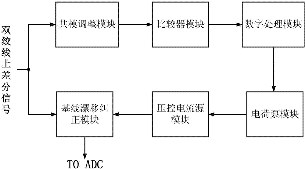
[0030] The high-pass characteristic of the isolation transformer will attenuate the DC and low-frequency components of the signal, causing the baseline drift of the signal common-mode voltage. The baseline drift voltage correction circuit of the present invention corrects the baseline drift of the signal common-mode voltage by judging the degree of baseline drift of the received signal. Such as figure 1 As shown, the baseline drift voltage correction circuit of the present invention includes a common mode adjustment module, a comparator module, a digital processing module, a charge pump module, a voltage-controlled current source module and a baseline drift correction module.

[0031] Common mode adjustment module: Receive the differential signal input on the twisted pair, and perform common mode adjustment on it, that is, adjust the voltage of the differential signal from 2.5V to 1.25V, so that the differential signal is adjusted to the input range of the comparator, and the a...


PUM


Abstract

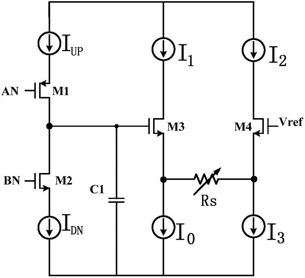
The invention discloses a baseline drift voltage correcting circuit used for an internet access chip. The baseline drift voltage correcting circuit comprises a common-mode adjusting module, a comparer module, a digital processing module, a charge pump module, a voltage-controlled current source module and a baseline drift correcting module. Input differential signals after passing through the common-mode adjusting module are adjusted to be within an input range of a comparer; the comparer compares the differential signals at a positive end and a negative end and outputs square waves; the digital processing module controls the charge pump module to output different control voltages based on the duty ratio of the square waves output by the comparer; and the control voltages control the volume of compensating current in a baseline drift module so as to finish correction for the baseline drift of the input signals. The baseline drift voltage correcting circuit determines and compensates signal DC and low-frequency attenuation caused by a high-pass characteristic of an isolation transformer, corrects the baseline drift in the signal transmission and improves the noise margin of the circuit. Meanwhile, the design difficulty of a simulation circuit is reduced, the dynamic input range of an ADC is no longer sacrificed, and the baseline drift voltage correction range of the circuit is enlarged.

Description

technical field [0001] The invention relates to a baseline drift voltage correction circuit for network port chips, belonging to the field of Ethernet baseband communication. Background technique [0002] In order to increase the signal transmission distance, improve the signal anti-interference ability, and be compatible with network ports with different interface levels, when the network port chip is used, the electrical port output needs to be equipped with an isolation transformer. However, the high-pass characteristics of the isolation transformer cause signal DC and low-frequency attenuation, resulting in baseline drift in signal transmission. As the length of the transmission line increases, the baseline drift in signal transmission will also increase, resulting in the system bit error rate. Increase and increase, so that the noise margin is seriously affected, and may cause the input of the subsequent ADC to exceed the allowable range. Therefore, the baseline drift v...

Claims


Application Information

Patent Timeline
IPC IPC(8): H03K19/0175
CPCH03K19/018507
Inventor 康晓飞周翰铭朱红董哲郭楹蒋敏强
Owner BEIJING MXTRONICS CORP
Learn More