Processing method of sheet-type fuse blocking layer
A processing method and barrier layer technology, applied in the manufacture of emergency protective devices, electrical components, fuses, etc., can solve the problems of lower product quality and pass rate, long time-consuming barrier layers, low personnel efficiency, etc., to improve product quality and The pass rate, the property of enhancing the resistance to physical shock, and the effect of increasing the accumulation speed
- Summary
- Abstract
- Description
- Claims
- Application Information
AI Technical Summary
Problems solved by technology
Method used
Image
Examples
Embodiment 1
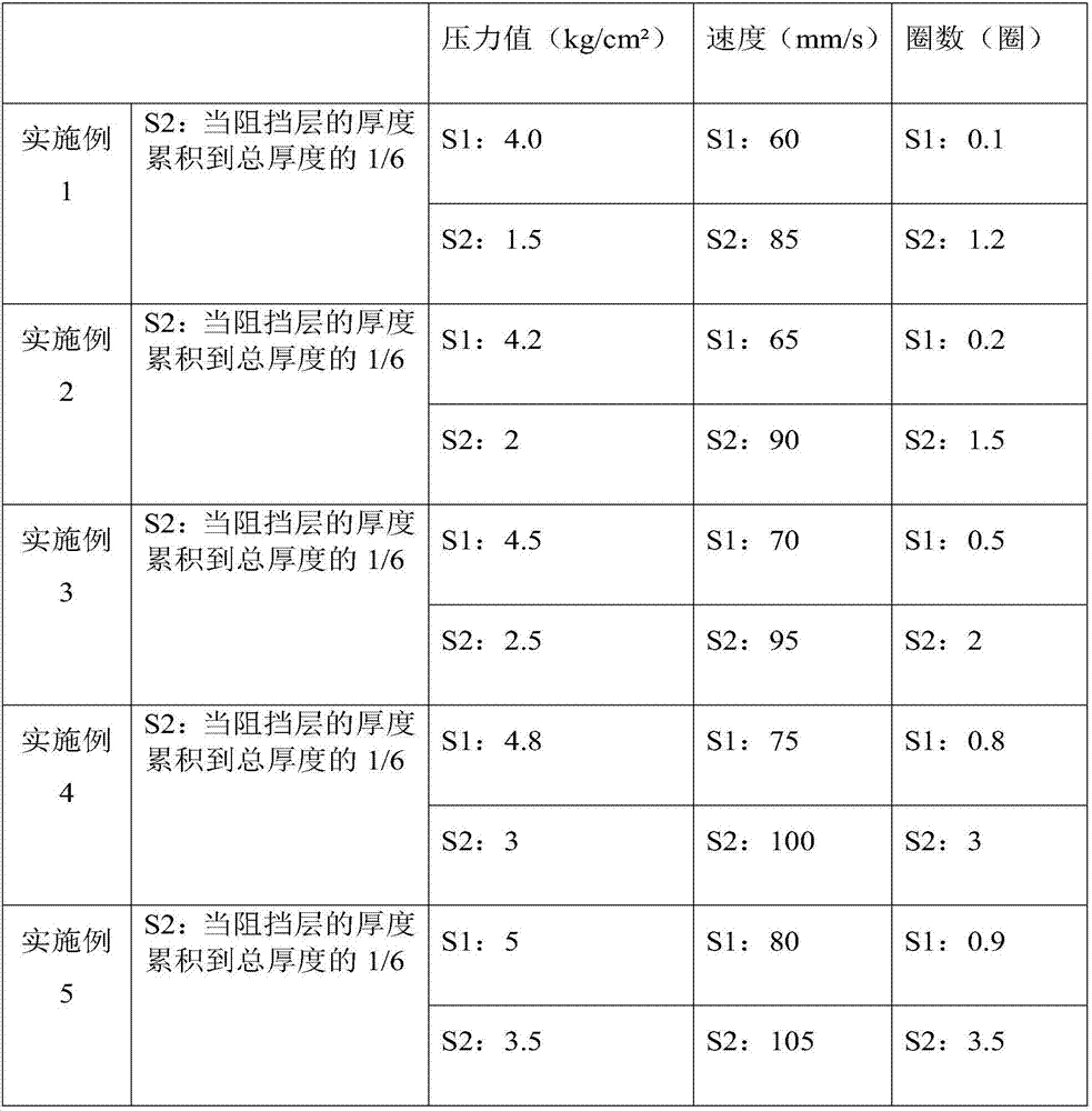
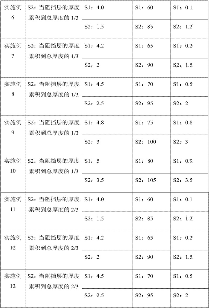
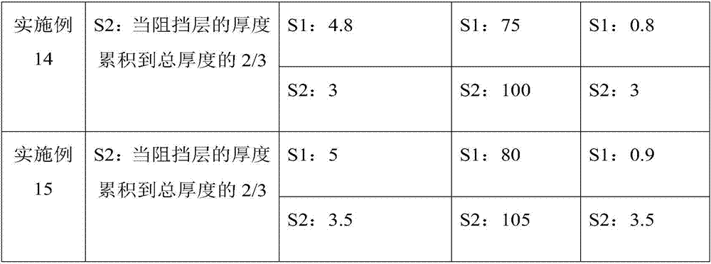
[0036] This embodiment provides a method for processing the barrier layer of a chip fuse, which includes the following steps:
[0037] S1: When printing the barrier layer, the pressure value is 4.0kg / cm 2 , the speed is 60mm / s, the number of turns is 0.1, and the printing is carried out;
[0038] S2: When the thickness of the barrier layer accumulates to 1 / 6 of the total thickness, the pressure value is 1.5kg / cm 2 , the speed is 85mm / s, and the number of turns is 1.2 turns for printing.
[0039] Wipe the screen with a dust-free paper every time the printing of the barrier layer of the chip fuse is completed for 3 pieces.
Embodiment 2
[0041] This embodiment provides a method for processing the barrier layer of a chip fuse, which includes the following steps:
[0042] S1: When printing the barrier layer, the pressure value is 4.2kg / cm 2 , The speed is 65mm / s, the number of turns is 0.2, and the printing is carried out;
[0043] S2: When the thickness of the barrier layer accumulates to 1 / 6 of the total thickness, the pressure value is 2kg / cm 2 , the speed is 90mm / s, and the number of turns is 1.5 turns for printing.
[0044] Wipe the screen with a dust-free paper every time the printing of the barrier layer of the chip fuse is completed for 3 pieces.
Embodiment 3
[0046] This embodiment provides a method for processing the barrier layer of a chip fuse, which includes the following steps:
[0047] S1: When printing the barrier layer, the pressure value is 4.5kg / cm 2 , the speed is 70mm / s, the number of circles is 0.5 circles, and the printing is carried out;
[0048] S2: When the thickness of the barrier layer accumulates to 1 / 6 of the total thickness, the pressure value is 2.5kg / cm 2 , the speed is 95mm / s, and the number of turns is 2 turns for printing.
[0049] Wipe the screen with a dust-free paper every time the printing of the barrier layer of the chip fuse is completed for 3 pieces.
PUM
 Abstract
Description
Claims
Application Information


