Processing method of barrier layer of chip fuse

A processing method and barrier layer technology, which is applied to electrical components, emergency protection devices, circuits, etc., can solve the problems of lower product quality and pass rate, long time-consuming barrier layer, and low personnel efficiency, so as to improve product quality and pass rate , enhance the properties of resistance to physical shocks, and increase the effect of accumulating speed

Active Publication Date: 2019-01-04
CHINA ZHENHUA GRP YUNKE ELECTRONICS
View PDF8 Cites 0 Cited by
  • Summary
  • Abstract
  • Description
  • Claims
  • Application Information

AI Technical Summary

Problems solved by technology

[0003] The purpose of the present invention is to provide a processing method for the barrier layer of a chip fuse to solve the problem that the time-consuming printing of the square-shaped barrier layer in the prior art is long, the efficiency of personnel is low, and the small The bumps are likely to cause the breakage of the barrier layer, reducing product quality and pass rate

Method used


Image

  • Processing method of barrier layer of chip fuse
  • Processing method of barrier layer of chip fuse
  • Processing method of barrier layer of chip fuse

Examples


Embodiment 1

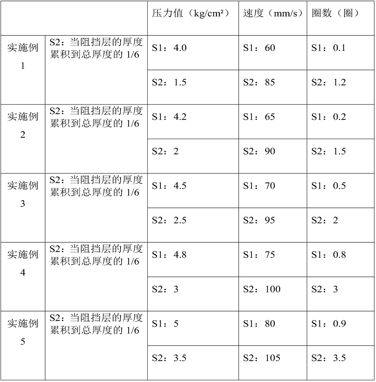
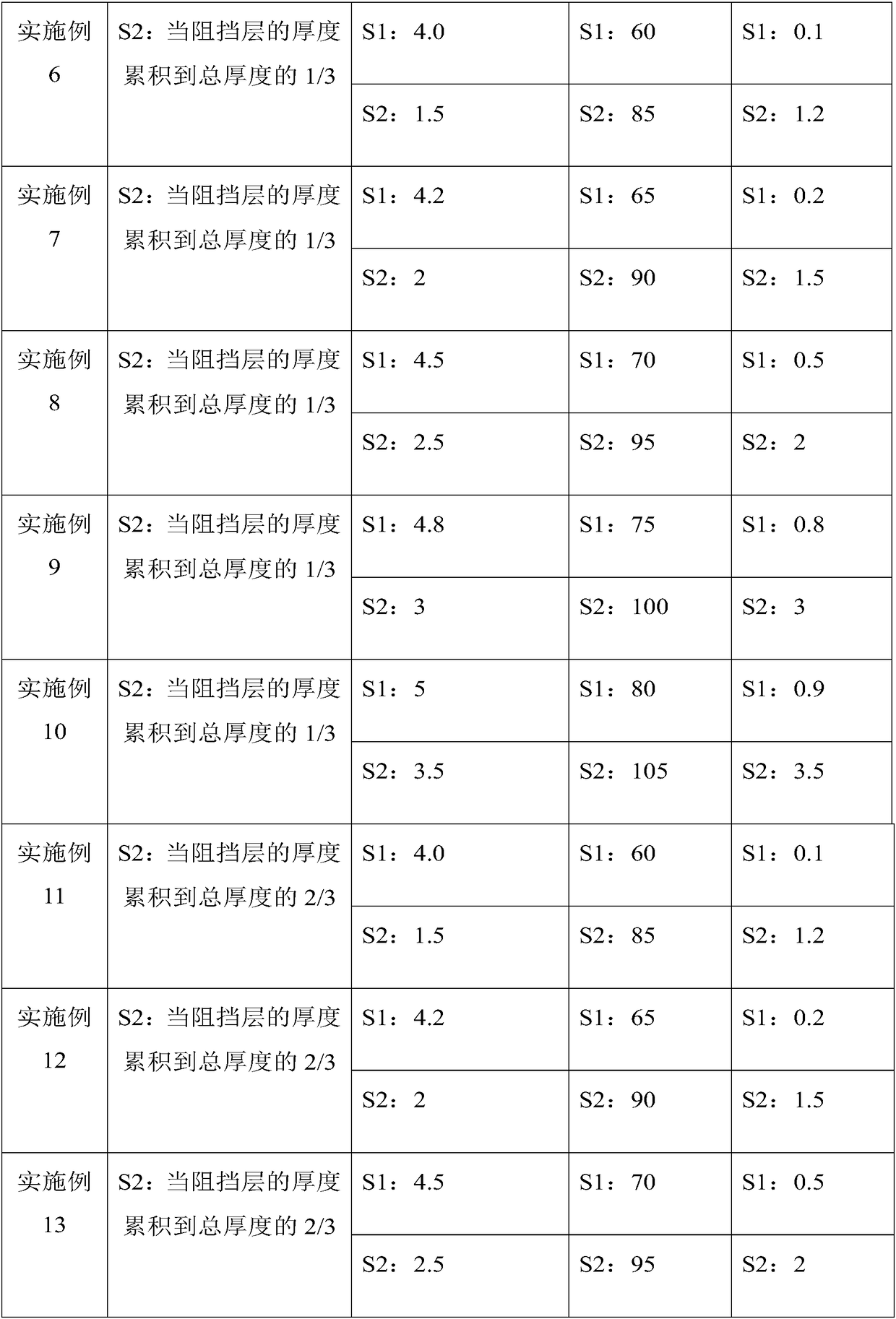
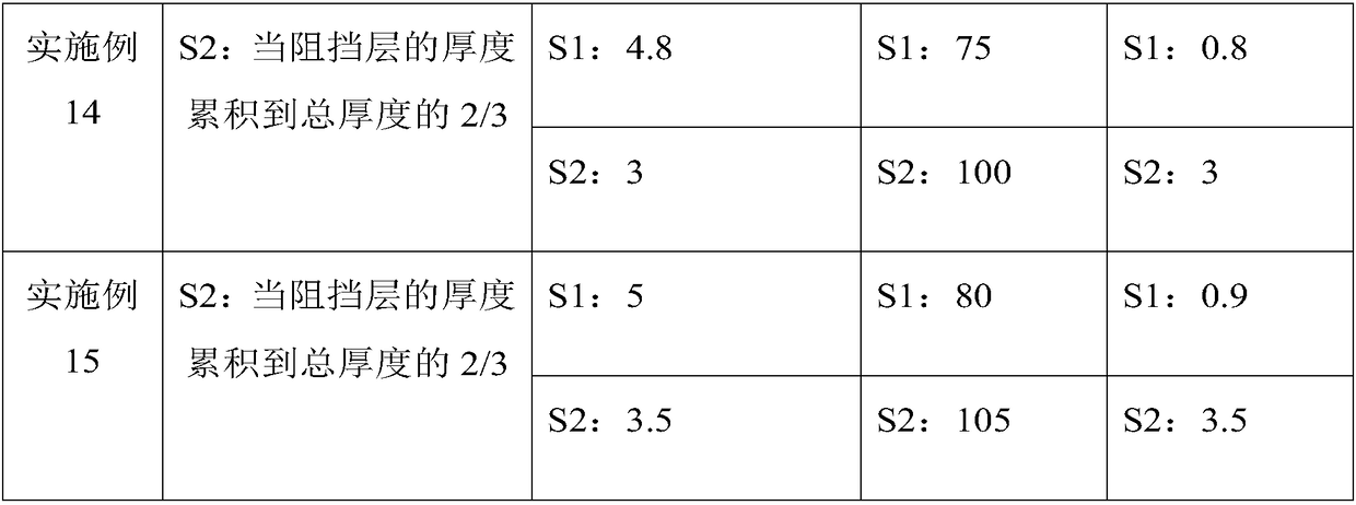
[0036] This embodiment provides a method for processing the barrier layer of a chip fuse, which includes the following steps:

[0037] S1: When printing the barrier layer, the pressure value is 4.0kg / cm 2 , the speed is 60mm / s, the number of turns is 0.1, and the printing is carried out;

[0038] S2: When the thickness of the barrier layer accumulates to 1 / 6 of the total thickness, the pressure value is 1.5kg / cm 2 , the speed is 85mm / s, and the number of turns is 1.2 turns for printing.

[0039] Wipe the screen with a dust-free paper every time the printing of the barrier layer of the chip fuse is completed for 3 pieces.

Embodiment 2

[0041] This embodiment provides a method for processing the barrier layer of a chip fuse, which includes the following steps:

[0042] S1: When printing the barrier layer, the pressure value is 4.2kg / cm 2 , The speed is 65mm / s, the number of turns is 0.2, and the printing is carried out;

[0043] S2: When the thickness of the barrier layer accumulates to 1 / 6 of the total thickness, the pressure value is 2kg / cm 2 , the speed is 90mm / s, and the number of turns is 1.5 turns for printing.

[0044] Wipe the screen with a dust-free paper every time the printing of the barrier layer of the chip fuse is completed for 3 pieces.

Embodiment 3

[0046] This embodiment provides a method for processing the barrier layer of a chip fuse, which includes the following steps:

[0047] S1: When printing the barrier layer, the pressure value is 4.5kg / cm 2 , the speed is 70mm / s, the number of circles is 0.5 circles, and the printing is carried out;

[0048] S2: When the thickness of the barrier layer accumulates to 1 / 6 of the total thickness, the pressure value is 2.5kg / cm 2 , the speed is 95mm / s, and the number of turns is 2 turns for printing.

[0049] Wipe the screen with a dust-free paper every time the printing of the barrier layer of the chip fuse is completed for 3 pieces.


PUM


Abstract

The invention relates to the field of electronic component manufacturing, and aims to solve the problems in the prior art that printing a square frame-shaped barrier layer takes a long time, the efficiency of personnel is low, the barrier layer is easy to break, and the product quality and pass rate are low. The processing method of the barrier layer of the type fuse. The processing method of the barrier layer of the chip fuse provided in the embodiment of the present invention first adopts the method of high pressure, low speed and low number of turns to ensure that the base of the barrier layer is smooth and smooth, and facilitates the accumulation of subsequent barrier layers. After printing, reduce the pressure, increase the speed, and increase the number of turns to print, and change the barrier layer from a trapezoidal shape with a narrow top and a wide bottom to a rectangular shape with the same width at the top and bottom, so as to enhance the physical impact resistance of the barrier layer and increase the accumulation speed of the barrier layer thickness. . The processing method for the barrier layer of the chip fuse provided in the embodiments of the present invention can effectively avoid the barrier layer from being easily broken, reduce production costs, and improve product quality and yield.

Description

technical field [0001] The invention relates to the field of manufacturing electronic components, in particular to a processing method for a barrier layer of a chip fuse. Background technique [0002] CFF / 6025 / F and CFF / 6332 / F chip fuses need to print a square frame barrier layer, and the thickness needs to be accumulated to 500-650μm according to the process requirements. According to the traditional printing method, not only is it time-consuming and the efficiency of personnel is low, but also small bumps when handling the substrate or during the printing process can easily cause the barrier layer to break, reducing product quality and pass rate. Contents of the invention [0003] The purpose of the present invention is to provide a processing method for the barrier layer of a chip fuse to solve the problem that the time-consuming printing of the square-shaped barrier layer in the prior art is long, the efficiency of personnel is low, and the small Any bumps are likely ...

Claims


Application Information

Patent Timeline
Patent Type & Authority Patents(China)
IPC IPC(8): H01H69/02
CPCH01H69/022
Inventor 肖晴韩玉成李厚忠刘应强彭昌文王成蒲蓉王海珍
Owner CHINA ZHENHUA GRP YUNKE ELECTRONICS
Why Eureka
Try Eureka