
Eureka
For R&D, Eureka makes reading and utilizing patents & technical documents easy.
Eureka AIR
Designed for self-driven R&D workflows. Generate viable solutions, solve complex R&D challenges, empower your innovation with AI.

Eureka Materials
Designed for material experts only. Revolutionize your material R&D, from search, analyze, to developing new materials.

TechResearch
Generate reliable direction feasibility study reports for your R&D in just a few steps.

TechSeek
Discover and master advanced knowledge NOW. Basics, ideas, possibilities, all at once.

TechMind
As an expert in R&D Theories, TechMind can generates customized viable solutions instantly.

TechRisk
Analyze your overall solution with one click, know your potential R&D risks in advance.

TechMonitor
Get weekly tech updates, stay abreast of the latest tech innovations and key insights.
Antireflection film and polycrystalline silicon solar cell
A technology of anti-reflection film and film layer, which is applied in the direction of circuits, photovoltaic power generation, electrical components, etc., and can solve the problems of high reflectivity and poor anti-PID performance
- Summary
- Abstract
- Description
- Claims
- Application Information
AI Technical Summary
Problems solved by technology
Method used
Image

Examples
Embodiment 1
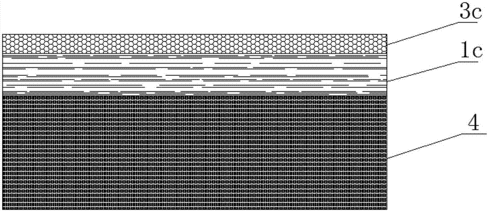
[0061] combine Figure 1 to Figure 3 As shown, the first embodiment provides an anti-reflection film, which at least includes a silicon nitride oxide film layer and a silicon nitride gradient film layer, and a laminated layer is formed between the silicon nitride oxide film layer and the silicon nitride gradient film layer. film structure. It can be seen that the film structure has the effect of reducing reflectivity and anti-PID performance. It can be understood that both the silicon oxynitride film layer and the silicon nitride graded film layer can be understood as a layered film structure with a certain thickness, and the anti-reflection film is formed by stacking these two layered film structures. Among them, the silicon nitride oxide film layer has the performance of anti-PID, and the silicon nitride gradient film layer has the effect of reducing the reflectivity.
[0062] In this embodiment, PECVD can be used for coating, and the silicon nitride oxide film layer and t...
Embodiment 2
[0065] combine figure 1 As shown, the second embodiment provides a further technical solution on the basis of the first embodiment.
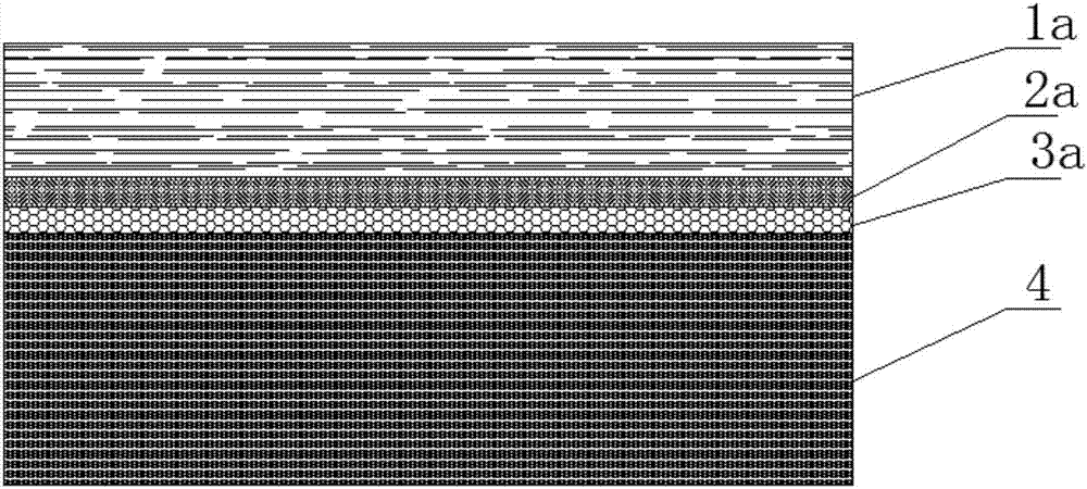
[0066] The antireflection film comprises a first silicon nitride oxide film layer 3a, a first silicon nitride film layer 2a and a first silicon nitride gradient film layer 1a; the first silicon nitride film layer 2a is deposited on the first silicon nitride oxide film layer On top of 3a, the first graded silicon nitride film layer 1a is deposited on the first silicon nitride film layer 2a. Of course, the first silicon oxynitride film layer 3 a will also be correspondingly deposited on the silicon substrate 4 during film coating. The anti-reflection film in this embodiment has a three-layer film structure, wherein the first silicon nitride oxide film layer 3a has the performance of anti-PID, the first silicon nitride gradient film layer 1a has the effect of reducing reflectivity, and the first silicon nitride film layer 3a has the effect of redu...
Embodiment 3
[0085] combine figure 2 As shown, the third embodiment provides a further technical solution on the basis of the first embodiment.
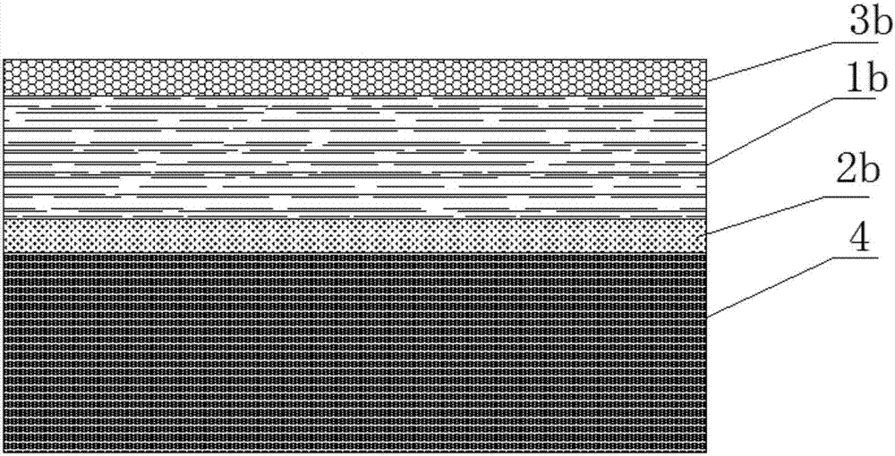
[0086] The antireflection film includes a second silicon nitride film layer 2b, a second silicon nitride gradient film layer 1b and a second silicon nitride oxide film layer 3b; the second silicon nitride gradient film layer 1b is deposited on the second silicon nitride film On the layer 2b, a second silicon nitride oxide film layer 3b is deposited on the second silicon nitride gradient film layer 1b. Of course, the second silicon nitride film layer 2b will also be correspondingly deposited on the silicon substrate 4 during film coating. The anti-reflection film in this embodiment has a three-layer film structure, wherein the second silicon nitride oxide film layer 3b has anti-PID performance, the second silicon nitride gradient film layer 1b has the effect of reducing reflectivity, and the second silicon nitride film layer 1b has the effect of...
PUM
| Property | Measurement | Unit |
|---|---|---|
| thickness | aaaaa | aaaaa |
| thickness | aaaaa | aaaaa |
| thickness | aaaaa | aaaaa |
Abstract
Description
Claims
Application Information
 - R&D Engineer
- R&D Manager
- IP Professional
- Industry Leading Data Capabilities
- Powerful AI technology
- Patent DNA Extraction
Browse by: Latest US Patents, China's latest patents, Technical Efficacy Thesaurus, Application Domain, Technology Topic, Popular Technical Reports.
© 2024 PatSnap. All rights reserved.Legal|Privacy policy|Modern Slavery Act Transparency Statement|Sitemap|About US| Contact US: help@patsnap.com