A kind of qled display device, preparation method and application

A display device, display technology, applied in the direction of semiconductor devices, electric solid devices, electrical components, etc., can solve the problems of reducing the current density of the hole transport layer, uneven QLED light emission, poor flatness of the hole transport layer, etc. Effect of electron transport capability, enhancement of QLED display brightness, and hole transport capability

Active Publication Date: 2019-12-31
HISENSE VISUAL TECH CO LTD
View PDF5 Cites 0 Cited by
  • Summary
  • Abstract
  • Description
  • Claims
  • Application Information

AI Technical Summary

Problems solved by technology

However, the use of a single inorganic metal oxide as the hole transport layer in the prior art will result in poor flatness of the hole transport layer, large surface impedance, poor coverage and poor film formation, which will reduce the current density of the hole transport layer, resulting in Uneven light emission of QLED

Method used


Image

  • A kind of qled display device, preparation method and application
  • A kind of qled display device, preparation method and application

Examples


preparation example Construction

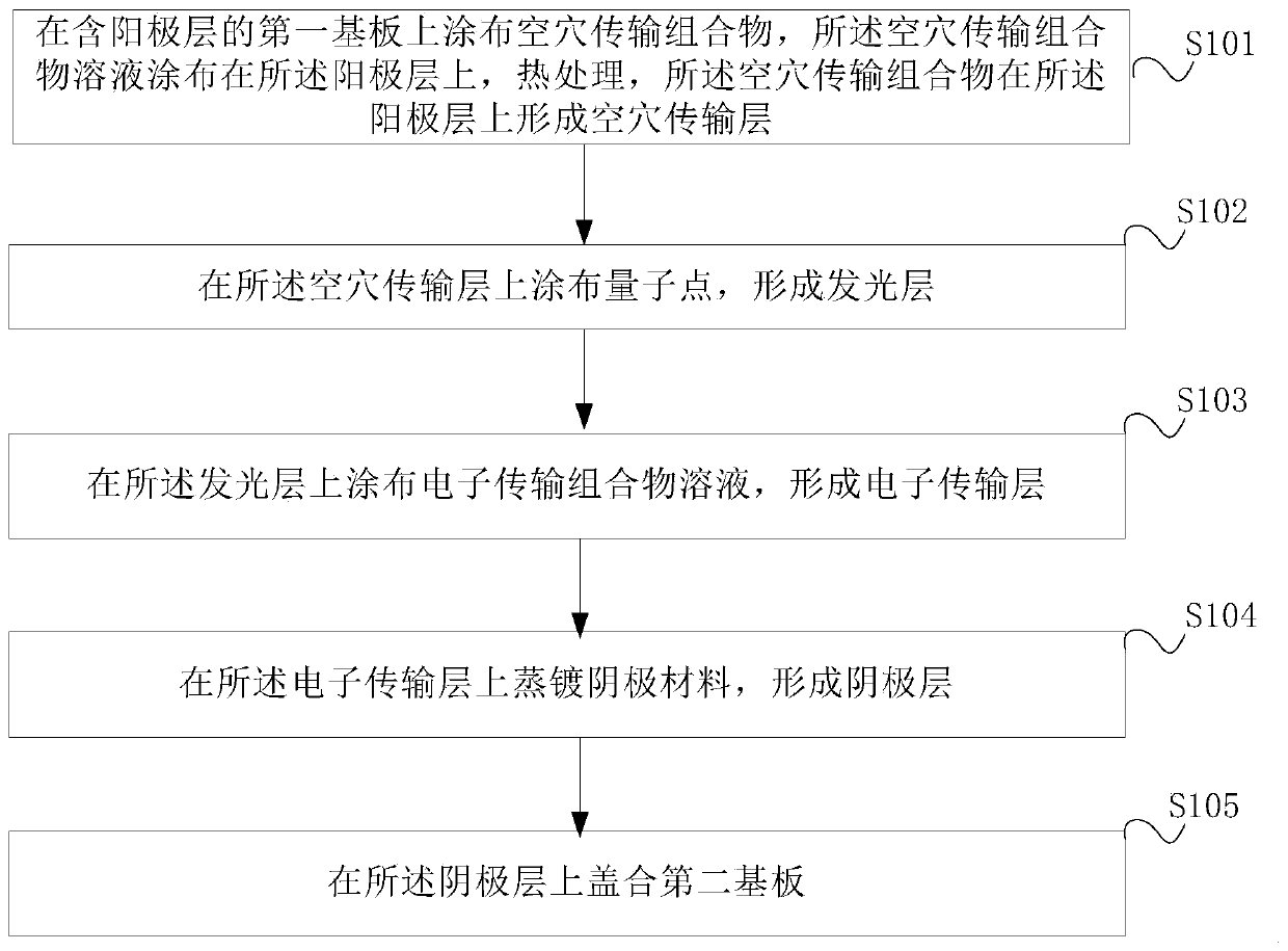
[0039] Please refer to the attached figure 2 , shows the flow chart of the method for preparing the QLED display device provided in the embodiment of the present application. attached by figure 2 As shown, the method includes the following steps:

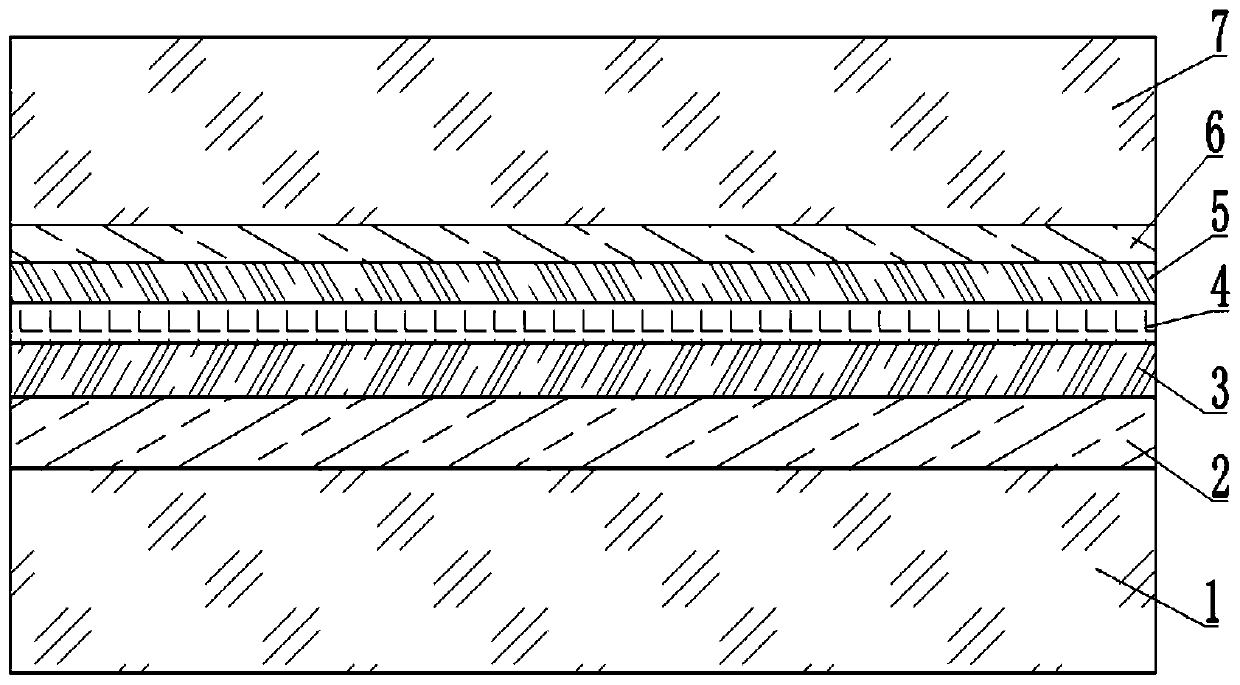
[0040] S101: Coating a hole transport composition on the first substrate containing an anode layer, the solution of the hole transport composition is coated on the anode layer, heat treatment, the hole transport composition is on the anode layer A hole transport layer is formed on it.

[0041] In this embodiment, the first substrate contains an anode layer, and the existing first substrate that has been coated with an anode layer can be selected, and the anode material can be coated or vacuum-plated on the first substrate after the first substrate is selected. on the substrate. The first substrate may be a rigid substrate or a flexible substrate. Specifically, the rigid substrate may be a glass substrate, and the flexible subs...

Embodiment 2

[0062] A method for preparing a QLED display device. On a glass substrate containing 110nm thick ITO, spin-coat an ethanol solution of a hole-transporting composition, and form a hole-transporting layer after heat treatment. The thickness of the hole-transporting layer is 50nm. Delivery compositions include WO 3 and NiO, WO 3 The average particle size of NiO is 2nm, the average particle size of NiO is 7nm, NiO and WO 3 The ratio of parts by weight is 0.8:1, the heat treatment temperature is 400°C, and the treatment time is 30 minutes; the quantum dot orthogonal liquid is spin-coated on the hole transport layer to form a 40nm light-emitting layer, and the quantum dots are CdS / ZnS; on the light-emitting layer Spin-coat the ethanol solution of electron transport composition, form electron transport layer after heat treatment, the thickness of electron transport layer is 50nm, electron transport composition comprises ZnO and TiO 2 , the average particle size of ZnO is 3nm, TiO ...

Embodiment 3

[0065] A kind of preparation method of QLED display device, on the glass substrate that contains 50nm thick ITO, the ethanol solution of hole transport composition is spin-coated, forms hole transport layer after heat treatment, and the thickness of hole transport layer is 60nm, hole Delivery compositions include WO 3 and NiO, WO 3 The average particle size of NiO is 2nm, the average particle size of NiO is 10nm, NiO and WO 3 The ratio of parts by weight is 0.9:1, the heat treatment temperature is 450°C, and the treatment time is 40 minutes; spin-coat quantum dot orthogonal liquid on the hole transport layer to form a 50nm light-emitting layer, and the quantum dots are CdS / ZnS; on the light-emitting layer Spin-coat the ethanol solution of electron transport composition, form electron transport layer after heat treatment, the thickness of electron transport layer is 40nm, electron transport composition comprises ZnO and TiO 2 , the average particle size of ZnO is 2nm, TiO 2 ...


PUM


Abstract

The invention discloses a QLED display device, a preparation method and an application. The QLED display device comprises a first substrate and a second substrate; a positive electrode layer, a hole transport layer, a light emitting layer, an electron transfer layer and a negative electrode layer are stacked between the first substrate and the second substrate in sequence, wherein the hole transport layer is prepared from a hole transport combination material; the hole transport combination material comprises at least two kinds of nano-metal oxides; the electron transfer layer is prepared from an electron transfer combination material; and the electron transfer combination material comprises at least two kinds of nano-metal oxides. By virtue of the QLED display device, the preparation method and the application provided by the invention, the optical conversion rate can be improved, and the QLED display luminance can be reinforced.

Description

technical field [0001] The present application relates to the technical field of liquid crystal televisions, in particular to a QLED display device, a preparation method and an application. Background technique [0002] QD (Quantum Dots) is a particle that emits colored light whenever it is stimulated by light or electricity. The light emission of QD has the advantages of high color purity, long life, and easy dispersion. QLED (Quantum Dot Light Emitting Diodes, Quantum Dot Light Emitting Diodes) makes full use of the luminous advantages of QD. It has the characteristics of high brightness, fast response, wide color gamut, and better HDR (High Data Rate, high dynamic lighting rendering) effect. It is generally considered to be the ultimate form of next-generation quantum display technology. [0003] QLED is generally a light-emitting device composed of a laminated anode layer, a hole transport layer, a QD light-emitting layer, an electron transport layer, and a cathode laye...

Claims


Application Information

Patent Timeline
Patent Type & Authority Patents(China)
IPC IPC(8): H01L33/14H01L33/00H01L27/15
CPCH01L27/15H01L33/0083H01L33/14
Inventor 刘振国宋志成刘卫东
Owner HISENSE VISUAL TECH CO LTD
Why Eureka
Try Eureka