Spherical pin element positioning algorithm based on point matching

A technology of pin components and positioning algorithm, applied in the direction of calculation, graphic image conversion, image data processing, etc., can solve the problem of lack of spherical pin chip position and angle, and achieve the effect of improving accuracy

Active Publication Date: 2017-12-22
HARBIN INST OF TECH
View PDF8 Cites 14 Cited by
  • Summary
  • Abstract
  • Description
  • Claims
  • Application Information

AI Technical Summary

Problems solved by technology

[0004] The present invention is to solve the existing problem of lacking the ability to accurately measure the position and angle of the ball pin chip

Method used


Image

  • Spherical pin element positioning algorithm based on point matching
  • Spherical pin element positioning algorithm based on point matching
  • Spherical pin element positioning algorithm based on point matching

Examples


specific Embodiment approach 1

[0022] Specific implementation mode one: refer to Figure 1 to Figure 5 Describe this embodiment in detail, a kind of positioning algorithm based on the spherical pin element of point matching described in this embodiment, this algorithm comprises the following steps:

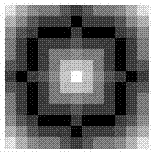
[0023] Step 1. According to the solder balls of the chip, the template image of the solder balls is obtained;

[0024] Step 2, performing edge detection on the chip image to obtain an edge image of the chip;

[0025] Step 3, using the template image obtained in step 1 as a core, performing correlation filtering on the edge image obtained in step 2 to obtain a filtered image;

[0026] Step 4: Count the number and position information of the pixel values ​​greater than the threshold pixel value in the filtered image in step 3, and obtain the coordinate set of the center positions of all solder balls in the chip image according to the statistical information

[0027] Step 5. According to the model information ...

specific Embodiment approach 2

[0034] Specific embodiment two: This embodiment is a further description of a positioning algorithm based on point-matching spherical pin components described in specific embodiment one. In this embodiment, in step five, the coordinates of the centers of all solder balls set , select the center coordinate set of the outermost solder ball of the chip and the coordinate set of the center coordinates of the outermost solder ball of the chip The specific process is:

[0035] Since the BGA chip solder balls are arranged in a matrix, the point with the smallest vertical coordinate of the solder ball center in the leftmost column (x 2 ,y 2 ) and the point with the largest ordinate (x 4 ,y 4 ), the point with the smallest vertical coordinate of the solder ball center in the rightmost column (x 0 ,y 0 ) and the point with the largest ordinate (x 6 ,y 6 ), the point with the smallest abscissa of the solder ball center on the uppermost row (x 3 ,y 3 ) and the point with the...

specific Embodiment approach 3

[0036]Specific embodiment three: This embodiment is a further description of a positioning algorithm based on point-matching spherical pin components described in specific embodiment one. In this embodiment, in step six, the coordinate set in step four is obtained and the center coordinate set of the outermost solder ball of the chip in step 5 The affine transformation of the matching point set The specific process is:

[0037] First calculate the center coordinate set of the outermost solder ball of the chip The distance between each coordinate point in the chip image, and then the coordinate set of all solder ball center positions in the chip image Search for a group of points with the closest distance between coordinate points, as an affine transformation matching point set


PUM


Abstract

The invention discloses a spherical pin element positioning algorithm based on point matching, which relates to the field of spherical pin element positioning. The spherical pin element positioning algorithm is disclosed to solve the problem of lack of accurate measurement of a position and an angle of a spherical pin chip at present. The spherical pin element positioning algorithm comprises the steps of: drawing a white circular image according to a radius size of a spherical pin and performing distance transformation; conducting edge detection on an original chip image and performing correlation filtering to obtain center coordinates of a solder ball point; selecting center coordinates of a solder ball at the peripheral endpoint of a chip for point matching, so as to obtain a rotary angle of the chip and deviation position coordinates of a chip entity center relative to the center of the chip image; fitting an edge image of the chip with a coordinate set shown in description by adopting a circle fitting method, so as to obtain a precise rotary angle of the chip and a precise deviation position coordinates of the chip entity center relative to the center of the chip image, thereby realizing the positioning of a spherical pin element. The spherical pin element positioning algorithm based on point matching is applied to the testing process of a spherical pin chip of a chip mounter.

Description

technical field [0001] The invention relates to a visual detection method for spherical pin components in a vision system of a placement machine, and mainly realizes the positioning function of the spherical pin components. Background technique [0002] With the development of the electronics industry, Surface Mount Technology (SMT, Surface Mount Technology) also develops rapidly. Among them, the placement machine is the key equipment of the SMT production line, which mainly realizes the placement of SMT components. The machine vision system of the placement machine directly affects the placement speed and accuracy of the placement machine, which puts forward high requirements for the visual recognition algorithm of components. [0003] In the existing vision system of the chip mounter, the visual detection accuracy of the spherical pin component is poor, and the position and angle of the ball pin chip cannot be accurately measured, so the positioning accuracy is poor. Co...

Claims


Application Information

Patent Timeline
Patent Type & Authority Applications(China)
IPC IPC(8): G01B11/00G01B11/26G06T7/13G06T7/73G06T3/00
CPCG01B11/002G01B11/26G06T3/0075G06T7/13G06T7/73G06T2207/20024
Inventor 杨宪强高会军白立飞张智浩孙光辉于金泳
Owner HARBIN INST OF TECH
Why Eureka
Try Eureka