A gate-controlled thyristor with high current rise rate

A high-current, thyristor technology, applied in the direction of circuits, electrical components, semiconductor devices, etc., can solve the problems of device surge current failure, inability to adjust the concentration distribution, etc., and achieve the effect of high current rise rate

Active Publication Date: 2019-12-10
UNIV OF ELECTRONICS SCI & TECH OF CHINA
View PDF5 Cites 0 Cited by
  • Summary
  • Abstract
  • Description
  • Claims
  • Application Information

AI Technical Summary

Problems solved by technology

The manufacturing process of traditional gate-controlled thyristors is based on the triple diffusion process of DMOS technology. Since the P well and N well on the cathode side are formed by implantation and diffusion, their concentration is limited by the forward conduction capability and withstand voltage requirements of the device. In the manufacturing process It is impossible to adjust the concentration distribution according to the high on-state current critical rise rate di / dt characteristic
Therefore, there is an urgent need for a device that can improve the high current rise characteristics, and then solve the problem that the device fails due to the inability to quickly discharge the surge current.

Method used


Image

  • A gate-controlled thyristor with high current rise rate
  • A gate-controlled thyristor with high current rise rate
  • A gate-controlled thyristor with high current rise rate

Examples


Embodiment

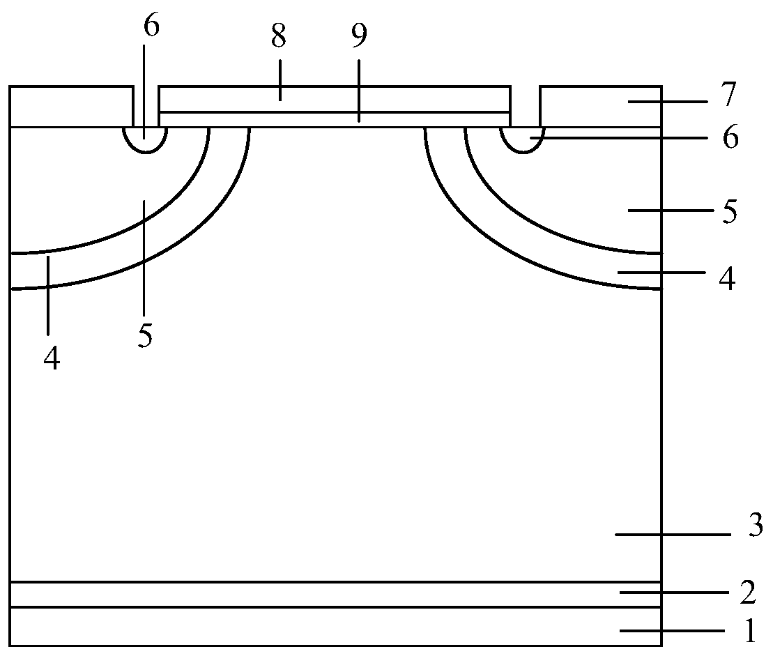
[0016] Such as figure 1 As shown, this embodiment provides a gate-controlled thyristor with a high current rise rate, comprising a first conductivity type semiconductor doped substrate 2 and a metal anode disposed on the back of the first conductivity type semiconductor doped substrate 2 1. The second conductivity type semiconductor doped epitaxial layer 3 is arranged on the front surface of the first conductivity type semiconductor doped substrate 2, and the top surface of the second conductivity type semiconductor doped epitaxial layer 3 is provided with a metal cathode 7 and An insulated gate, wherein the insulated gate is located in the middle, and the metal cathode 7 is located on both sides of the insulated gate and isolated therefrom; the insulated gate includes a gate dielectric layer 9 and a polysilicon gate 8 arranged on the upper surface of the gate dielectric layer 9; Two conductive type semiconductor doped epitaxial layers 3 are respectively provided with a first c...


PUM


Abstract

The invention provides a gate-controlled thyristor with a high current rising rate, which belongs to the technical field of power devices. The present invention includes a metal anode, a first conductivity type semiconductor doped substrate, and a second conductivity type semiconductor doped epitaxial layer stacked in sequence from bottom to top, and the upper surface of the second conductivity type semiconductor doped epitaxial layer is provided with A metal cathode and an insulating gate, the two ends of the top layer of the second conductivity type semiconductor doped epitaxial layer are respectively provided with the first conductivity type semiconductor doped well region, the second conductivity type semiconductor doped well region and the first conductivity type semiconductor heavy In the doped region, the forbidden band width of the second conductivity type semiconductor doped well material is greater than the forbidden band width of the first conductive type semiconductor doped well material, and the forbidden band width of the first conductive type semiconductor doped well material is greater than that of the first conductive type semiconductor doped well material. The forbidden band width of the doped epitaxial layer of the two-conductivity type semiconductor. Based on the device structure of the invention, the current rising rate of the gate-controlled thyristor can be greatly improved.

Description

Technical field [0001] The invention belongs to the technical field of power devices, and specifically relates to a gate-controlled thyristor with a high current rise rate. Background technique [0002] Capacitive energy storage has the advantages of stable energy storage, high power density and high transmission speed. In a pulsed power system with high instantaneous power, the energy supply of the system is usually provided by capacitive energy storage. The pulse width is determined by the time constant of the circuit. Therefore, the capacitive energy storage requires a sufficiently low load impedance to generate short pulses and large currents to achieve high current rise rates in pulsed power systems. Traditional switching devices such as spark gaps have the disadvantages of low switching rate, short service life and low efficiency, while solid-state switching devices have been used in pulsed power systems due to their superior portability, low cost and high efficiency. The ...

Claims


Application Information

Patent Timeline
Patent Type & Authority Patents(China)
IPC IPC(8): H01L29/744H01L29/06
CPCH01L29/0603H01L29/0611H01L29/0684H01L29/744
Inventor 李泽宏林育赐谢驰罗蕾李佳驹任敏张波
Owner UNIV OF ELECTRONICS SCI & TECH OF CHINA
Why Eureka
Try Eureka