Etching method, process equipment, thin film transistor device and manufacturing method thereof

A manufacturing method and technology of process equipment, applied in semiconductor/solid-state device manufacturing, semiconductor devices, electric solid-state devices, etc., can solve problems such as poor adhesion, improve product yield and product performance, and solve the effect of drilling and engraving problems.

Inactive Publication Date: 2020-04-17
BOE TECH GRP CO LTD +1
View PDF5 Cites 0 Cited by
  • Summary
  • Abstract
  • Description
  • Claims
  • Application Information

AI Technical Summary

Problems solved by technology

However, due to the poor adhesion of the photoresist on some materials, when these materials are etched, the photoresist will produce tiny gaps at the interface with the material to be etched, making the etching Etchants can easily drill into these tiny gaps and cause drilling

Method used


Image

  • Etching method, process equipment, thin film transistor device and manufacturing method thereof
  • Etching method, process equipment, thin film transistor device and manufacturing method thereof
  • Etching method, process equipment, thin film transistor device and manufacturing method thereof

Examples


Embodiment Construction

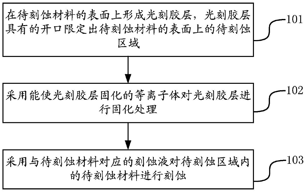
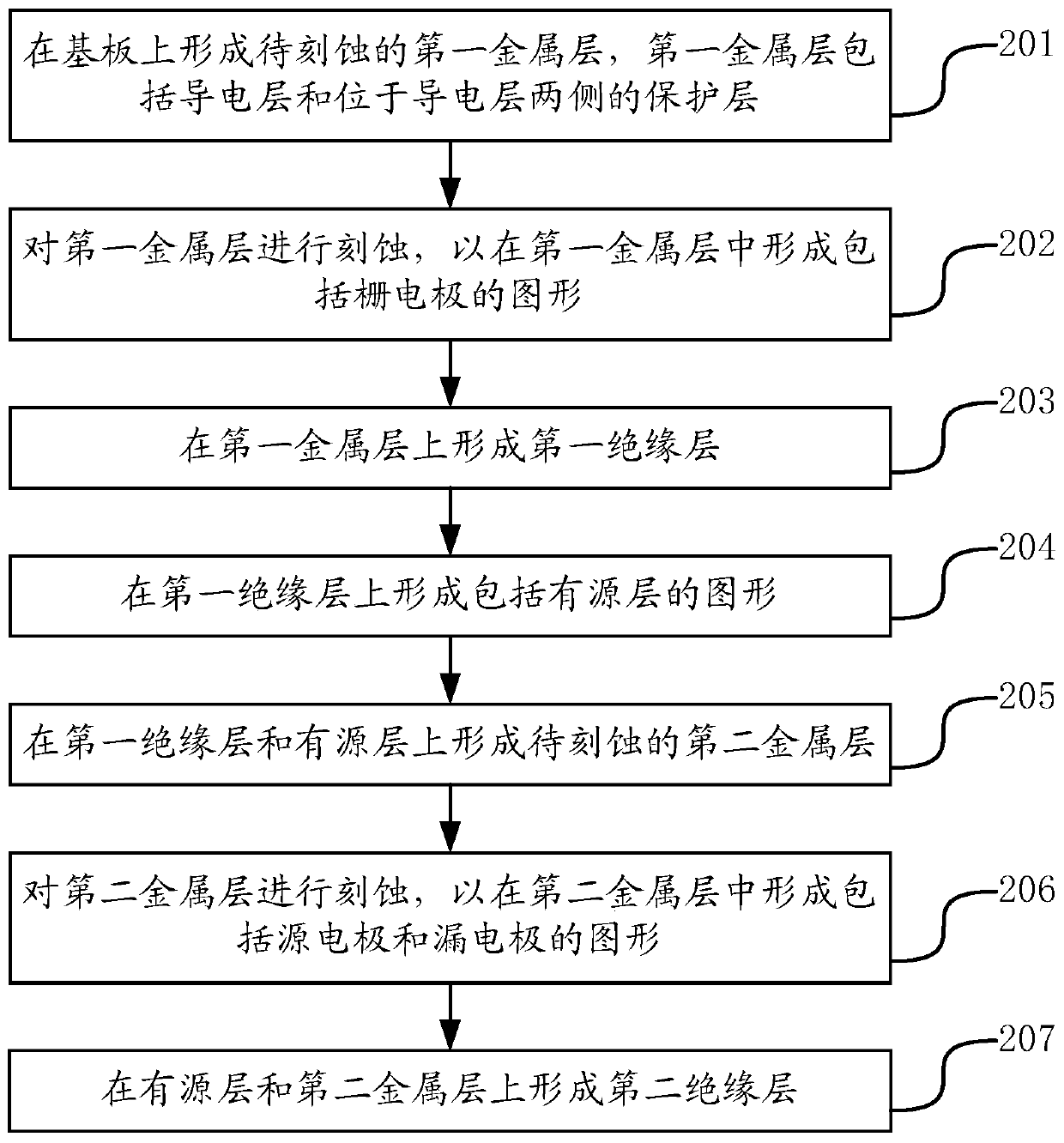
[0046] In order to make the object, technical solution and advantages of the present invention clearer, the implementation manner of the present invention will be further described in detail below in conjunction with the accompanying drawings. Apparently, the described embodiments are some, not all, embodiments of the present invention. Based on the described embodiments of the present invention, all other embodiments obtained by persons of ordinary skill in the art without creative efforts shall fall within the protection scope of the present invention. Unless otherwise defined, the technical terms or scientific terms used in the present invention shall have the usual meanings understood by those skilled in the art to which the present invention belongs. "First", "second" and similar words used in the present invention do not indicate any order, quantity or importance, but are only used to distinguish different components. "Comprising" or similar words mean that the elements...


PUM


Abstract

The invention discloses an etching method, process equipment, a thin film transistor device and a manufacturing method thereof, belonging to the field of semiconductor manufacturing. The etching method includes: forming a photoresist layer on the surface of the material to be etched, and the openings of the photoresist layer limit the area to be etched on the surface of the material to be etched; The cured plasma cures the photoresist layer; the material to be etched in the region to be etched is etched using an etching solution corresponding to the material to be etched. The present invention innovatively applies the plasma process commonly used in dry etching to wet etching, and in turn utilizes the fact that the photoresist in dry etching is easy to denature after being exposed to plasma and is difficult to be stripped Disadvantages, use plasma to enhance the contact between the photoresist layer and the material to be etched before the etchant reacts with the material to be etched, which solves the drilling problem caused by this, and helps to improve product yield and Product performance.

Description

technical field [0001] The invention relates to the field of semiconductor manufacturing, in particular to an etching method, process equipment, a thin film transistor device and a manufacturing method thereof. Background technique [0002] Etching (Etch) is a semiconductor manufacturing process and an important step in the microelectronics manufacturing process and micro-nano manufacturing process. It refers to the process of stripping and removing materials by means such as solutions, reactive ions or machinery. At present, it mainly includes two kinds of wet etching (Wet Etch, WE) and dry etching (Dry Etch, DE). When etching is used to pattern materials, photoresist can be used to cover the surface of a part of the material because it is easy to form a specified pattern by light, so that etching is only performed on the surface of the material that is not covered , so as to use the design of the photoresist pattern to realize the patterning of the material. However, due...

Claims


Application Information

Patent Timeline
Patent Type & Authority Patents(China)
IPC IPC(8): H01L21/027H01L21/28H01L21/311H01L29/66
CPCH01L21/0273H01L21/31058H01L21/32134H01L21/32139H01L27/1288H01L21/28H01L29/66H01L27/1266
Inventor 杜生平苏同上黄正峰杨玉张旺王磊马云刘丽华刘广东郭稳
Owner BOE TECH GRP CO LTD
Why Eureka
Try Eureka