
Preparation method of stencil printing mesh and preparation method for front-surface electrode of crystalline silicon solar cell

A technology of solar cells and front electrodes, applied in circuits, electrical components, semiconductor devices, etc., can solve problems such as uneven tension and uneven thickness, and achieve the effects of improving stability, improving life, and avoiding damage

Inactive Publication Date: 2018-01-09
JIANGSU SHUNFENG PHOTOVOLTAIC TECH CO LTD
View PDF8 Cites 1 Cited by
  • Summary
  • Abstract
  • Description
  • Claims
  • Application Information

AI Technical Summary

Problems solved by technology

[0007] In order to overcome the above-mentioned shortcoming of stencil printing, the present invention specially designs a set of stencil printing screen and its preparation method, and provides a method of using the stencil printing screen to prepare the front electrode of crystalline silicon solar cells, which solves the problems caused by thin grid lines. Problems of uneven tension and uneven thickness caused by length and scrape coating damage

Method used


Image

  • Preparation method of stencil printing mesh and preparation method for front-surface electrode of crystalline silicon solar cell
  • Preparation method of stencil printing mesh and preparation method for front-surface electrode of crystalline silicon solar cell
  • Preparation method of stencil printing mesh and preparation method for front-surface electrode of crystalline silicon solar cell

Examples


Embodiment

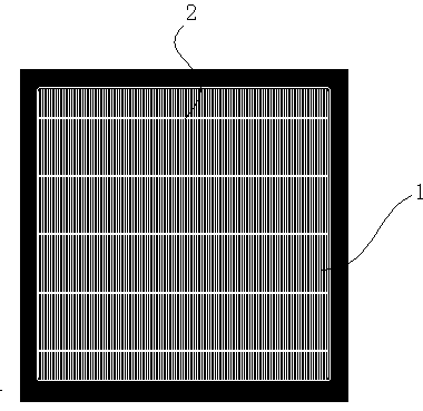
[0040] Example: such as figure 1As shown, the front electrode of a crystalline silicon solar cell with a silicon wafer size of 156*156mm is produced, wherein the total length of the auxiliary grid lines 1 is 150.5mm, and the number of auxiliary grid lines 1 is 97. The opening design of the auxiliary grid lines The width is 25um, and the number of busbar lines 2 is five.

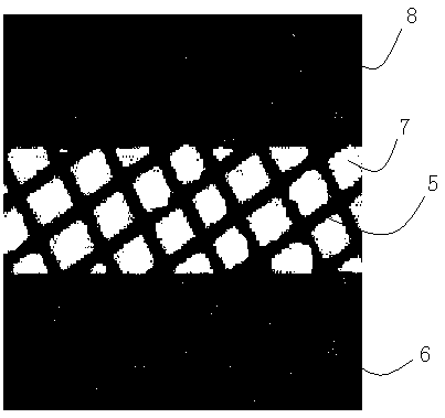
[0041] Such as Figure 4 with Figure 5 with Image 6 As shown, two stencil printing screens of plate A and plate B are preferred, and the production process is as follows:

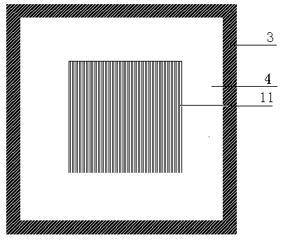
[0042] a) provide two stainless steel sheets 4 with the same size, thickness and structure, and a metal frame 3 is provided around the stainless steel sheets 4;

[0043] b) Outline the graphic of the corresponding front electrode of the crystalline silicon solar cell that needs to be manufactured. The opening width of the auxiliary grid line in the graphic is designed to be 21um, which is slightly smaller than the opening design widt...


PUM

PropertyMeasurementUnit
Diameteraaaaaaaaaa
Thicknessaaaaaaaaaa

Abstract

The invention belongs to the technical field of a photovoltaic assembly, and particularly relates to a preparation method of a stencil printing mesh and a preparation method for a front-surface electrode of a crystalline silicon solar cell. The method for preparing the stencil printing mesh comprises the following steps of providing two stainless steel thin sheets; equally dividing an auxiliary grid line according to an auxiliary grid line structure, and separating auxiliary grid line segments at intervals to form two patterns A and B; and respectively forming auxiliary grid line grooves corresponding to the pattern A and the pattern B and a plurality of round holes in the two stainless steel thin sheets so as to form a plate A and a plate B. The preparation method for the front-surface electrode of the crystalline silicon solar cell comprises the step of respectively and separately performing printing and combination on a solar cell to from a complete fine grid line structure and a complete main grid line structure by employing the plate A and the plate B and by a stencil printing process according to the formed plate A and the plate B. By the method, the defects that a conventional stencil printing plate is large in tension change, the morphology of the grid lines is changed and the stencil printing plate is not stable are ingeniously overcome, the service lifetime of the solar cell is greatly prolonged, the conversion efficiency of the solar cell is greatly improved, and the stencil printing mesh has remarkable characteristic.

Description

technical field [0001] The invention belongs to the technical field of photovoltaic modules, and in particular relates to a method for preparing a steel plate printing net and a method for preparing a front electrode of a crystalline silicon solar cell by using the steel plate printing net. Background technique [0002] At present, with the continuous development of crystalline silicon solar cell technology, while pursuing low cost, the industry has higher and higher requirements for the performance of solar cells, and higher requirements have been put forward for the conversion efficiency of solar cells and the cost of crystalline silicon solar cells. requirements. [0003] The manufacture of crystalline silicon solar cells mainly includes the following steps: 1. Silicon wafer cleaning and texturing; 2. Diffusion junction; 3. Anti-reflection coating; 4. Screen printing; 5. High temperature sintering to form metal contacts. Among them, the screen printing process is to make...

Claims


Application Information

Patent Timeline
IPC IPC(8): H01L31/0224
Inventor 瞿辉徐春曹玉甲张强
Owner JIANGSU SHUNFENG PHOTOVOLTAIC TECH CO LTD
Learn More