Roll-to-roll capacitive touch screen sensor and preparation method thereof
A capacitive touch screen, roll-to-roll technology, applied in the direction of electrical digital data processing, instruments, data processing input/output process, etc., can solve the problems of high energy consumption, inability to realize rapid manufacturing of touch screens, high processing costs, etc., to achieve conductive Good performance, good product performance stability, and low production cost
- Summary
- Abstract
- Description
- Claims
- Application Information
AI Technical Summary
Problems solved by technology
Method used
Image
Examples
preparation example Construction
[0052] The preparation method of above-mentioned first conductive ink, comprises:
[0053] Premixing step: dissolving the conductive polymer in the solvent, and then adding the silane coupling agent under stirring condition to completely dissolve the silane coupling agent to obtain a premixed solution;
[0054] The step of activating the nano-silver wire: adding a wetting and dispersing agent to the nano-silver wire, dispersing and activating the nano-silver wire, the concentration of the nano-silver wire in the solvent is 1-100mg / mL, and obtaining a nano-silver wire dispersion;
[0055] The step of dispersing the nano-metal particles: dispersing the nano-metal particles into a solvent to obtain a nano-metal particle dispersion;
[0056] Mixing step: add a pH regulator to adjust the pH of the premix to 7-8, add a polymer resin to the premix under agitation, and dissolve the polymer resin; then gradually add a viscosity regulator, non-ionic Surfactant, leveling agent and defoa...
Embodiment 1
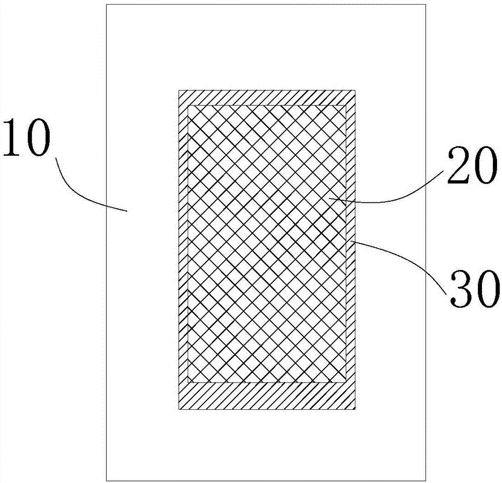
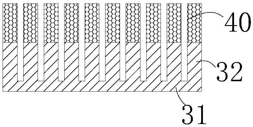
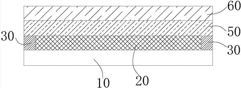
[0098] refer to Figure 1-Figure 3 , a roll-to-roll capacitive touch screen functional sheet, comprising a substrate 10, a first electrode 20, a second electrode 30, a third electrode 40, an erasure protection layer 50 and an OCA optical adhesive layer 60;
[0099] The first electrode 20 is disposed in the middle of the upper surface of the substrate 10;
[0100] The second electrode 30 is arranged on the upper surface of the substrate 10 and is located on the outer periphery of the first electrode 20; the second electrode 30 includes a second electrode body 31 connected to the first electrode 20 and a Several second electrode leads 32 extending outward from the second electrode body 31;
[0101] Each of the second electrode leads 32 is covered with the third electrode 40;
[0102] The erasure protection layer 50 covers the upper surface of the first electrode 20 , and the erasure protection layer 50 covers parts of the second electrode 30 other than the surface covered by t...
Embodiment 2
[0114] A roll-to-roll capacitive touch screen functional sheet, the difference lies in: the thickness of the substrate is 125um. The square resistance of the first electrode is 60Ω / □, and its thickness is 400nm. The square resistance of the second electrode is 1Ω / □, and its thickness is 1um. The square resistance of the third electrode is 10Ω / □, and its thickness is 5um. The thickness of the erasing protective layer is 300nm; the thickness of the OCA optical adhesive layer is 5um.
[0115] Others are the same as in Example 1.
PUM
| Property | Measurement | Unit |
|---|---|---|
| Thickness | aaaaa | aaaaa |
| Square resistance | aaaaa | aaaaa |
| Thickness | aaaaa | aaaaa |
Abstract
Description
Claims
Application Information


