Capacitive touch screen functional chip, preparation method thereof, capacitive touch screen and electronic device

A capacitive touch screen and functional sheet technology, applied in the field of electronic devices and capacitive touch screen functional sheets, can solve the problems of inability to achieve arbitrary bending, complicated production process, high production cost, etc., and achieve good bonding strength, good conductivity, and simple structure Effect

Pending Publication Date: 2018-11-13
珠海纳金科技有限公司
View PDF2 Cites 2 Cited by
  • Summary
  • Abstract
  • Description
  • Claims
  • Application Information

AI Technical Summary

Problems solved by technology

[0004] In order to overcome the deficiencies of the prior art, one of the purposes of the present invention is to provide a capacitive touch screen functional sheet to solve the problem that the existing capacitive touch screen functional sheet cannot be bent arbitrarily and is difficult to be applied to a flexible touch screen. In addition, it can also Overcome the complex production process, high production cost, poor light transmittance, high resistance, and wear resistance of existing capacitive touch screen functional sheets

Method used


Image

  • Capacitive touch screen functional chip, preparation method thereof, capacitive touch screen and electronic device
  • Capacitive touch screen functional chip, preparation method thereof, capacitive touch screen and electronic device
  • Capacitive touch screen functional chip, preparation method thereof, capacitive touch screen and electronic device

Examples


Embodiment 1

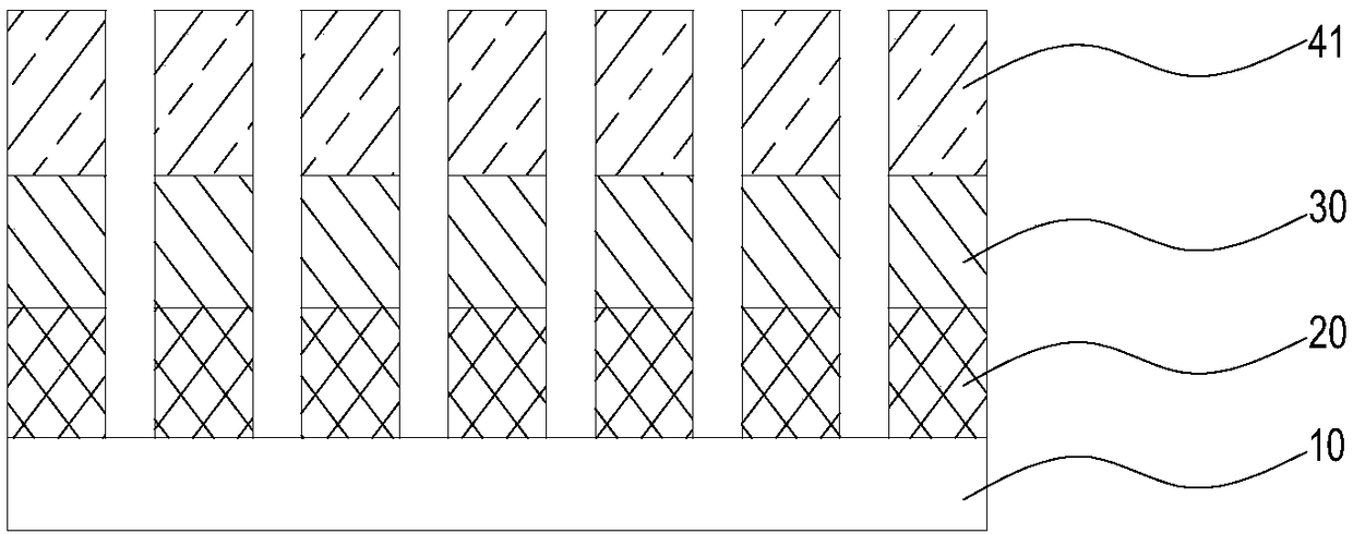
[0052] Printing step: by gravure printing method, on a 12 μm thick PET substrate (in this embodiment, the PET substrate is subjected to double-sided coating hardening treatment, so that the hardness of the printing surface is 1H, and the hardness of the non-printing surface is 3H). Roll printing of 30nm thick nano silver wire film layer, 10nm thick epoxy acrylic resin protective layer, 200nm thick nano silver particle conductive ink and 1μm thick graphene conductive ink, each printed layer needs to be dried and cured Only then can the next step of printing be carried out. Nano-silver particle conductive ink comprises a body layer and a lead layer extending outward from the body layer, the epoxy acrylic resin protective layer covers the nano-silver film layer, the body layer and the lead layer are all arranged on the epoxy acrylic resin protective layer, and the body The layer is located at the outer edge of the silver nanowire film layer, and the graphene conductive ink covers...

Embodiment 2

[0057] Printing process: by silk screen method, on the 2000μm thick polyvinyl chloride substrate (in this embodiment, the non-printing surface is subjected to single-side coating hardening treatment, so that its hardness is 3H) and sequentially print 2000nm thick nano Silver wire film layer, 300nm thick alkyd resin protective layer, 20000nm thick graphene conductive ink and 20μm thick silver copper powder conductive ink, each printed layer needs to be dried and cured before the next step of printing. The graphene conductive ink includes a body layer and a lead layer extending outward from the body layer. The alkyd resin protective layer covers the nano-silver film layer. Both the body layer and the lead layer are arranged on the alkyd resin protective layer, and the body layer is located At the outer edge of the silver wire film layer, silver-copper powder conductive ink covers the lead wire layer to obtain a printed board.

[0058] Etching step: laser etching out the capaciti...

Embodiment 3

[0062]Printing process: by jet printing method, on the 50μm thick polyimide substrate, roll-to-roll printed 80nm thick nano-silver wire film layer, 100nm thick phenolic resin protective layer, 5000nm thick silver powder-copper powder conductive ink And 5μm thick nano-titanium dioxide particle conductive ink, each printed layer needs to be dried and cured before the next step of printing. The silver powder-copper powder conductive ink includes a body layer and a lead layer extending outward from the body layer. The phenolic resin protective layer covers the nano silver wire film layer. The body layer and the lead layer are both arranged on the phenolic resin protective layer, and the body layer is located on the At the outer edge of the nano-silver wire film layer, the conductive ink of nano-titanium dioxide particles covers the lead layer to obtain a printing plate.

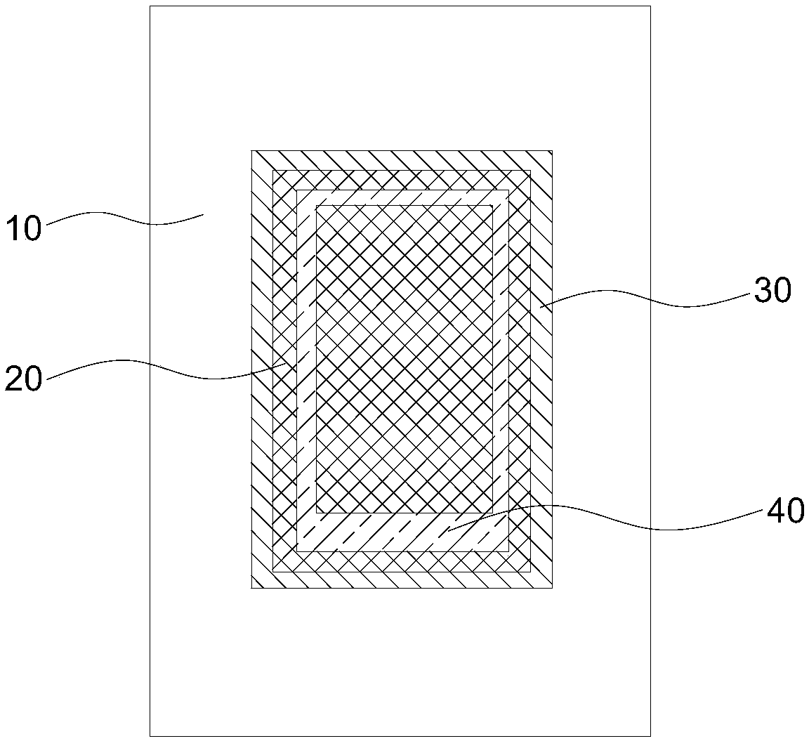
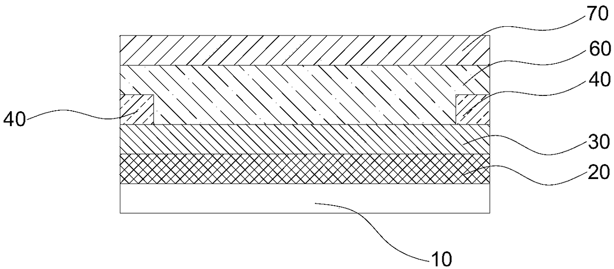
[0063] Etching step: laser etching out the capacitive sensing layer 20 on the nano-silver wire film layer, and...


PUM


Abstract

The invention discloses a capacitive touch screen functional chip, comprising a substrate, a capacitive sensing layer, a protection layer of the capacitive sensing layer, a conductive electrode layer,a wear-resistant conductive layer, a shadow elimination protection layer and an OCA optical adhesive layer, wherein the conductive electrode layer comprises a conductive electrode main body and a conductive electrode lead extending outward from the conductive electrode main body, and the capacitive sensing layer, the protection layer of the capacitive sensing layer, the shadow elimination protection layer and the OCA optical adhesive layer are transparent. The invention further discloses a preparation method of the capacitive touch screen functional chip, a capacitive touch screen and an electronic device. The capacitive touch screen functional chip disclosed by the invention has the advantages of good bending property, low resistance, good conductivity, high light transmittance, simple structure, etc.

Description

technical field [0001] The invention relates to the technical field of capacitive touch screens, in particular to a capacitive touch screen functional sheet, a method for preparing the capacitive touch screen functional sheet, a capacitive touch screen including the capacitive touch screen functional sheet, and an electronic device including the capacitive touch screen. Background technique [0002] With the increasing material level, consumers' requirements for electronic products are rapidly developing in terms of thinner, lighter, more flexible, visualized, and touch-sensitive devices. At present, touch screens and related industrial chains all over the world are being integrated into people's daily life at an extremely fast speed. In addition, flexible display technology shows that the display has the characteristics of being able to bend or curl into any shape, and has the characteristics of being light, thin and easy to carry. [0003] In the existing industry, hard i...

Claims


Application Information

Patent Timeline
Patent Type & Authority Applications(China)
IPC IPC(8): G06F3/044
CPCG06F3/044G06F2203/04102
Inventor 雷震丁轶钟江贵吴浩松
Owner 珠海纳金科技有限公司
Why Eureka
Try Eureka