A kind of shift register, gate drive circuit and display device

A technology for shift registers and drive signals, which can be used in static memory, digital memory information, instruments, etc., and can solve problems such as poor shift registers

Active Publication Date: 2021-09-14
BOE TECH GRP CO LTD +1
View PDF8 Cites 0 Cited by
  • Summary
  • Abstract
  • Description
  • Claims
  • Application Information

AI Technical Summary

Problems solved by technology

[0004] In view of this, an embodiment of the present invention provides a shift register, a gate drive circuit and a display device to solve the disadvantages of the existing shift register

Method used


Image

  • A kind of shift register, gate drive circuit and display device
  • A kind of shift register, gate drive circuit and display device
  • A kind of shift register, gate drive circuit and display device

Examples


Embodiment 1

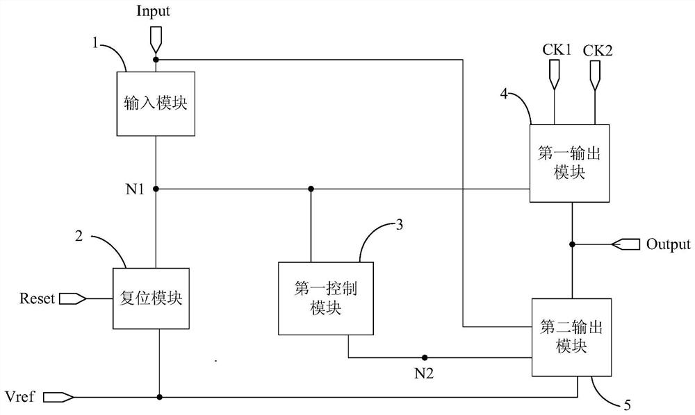
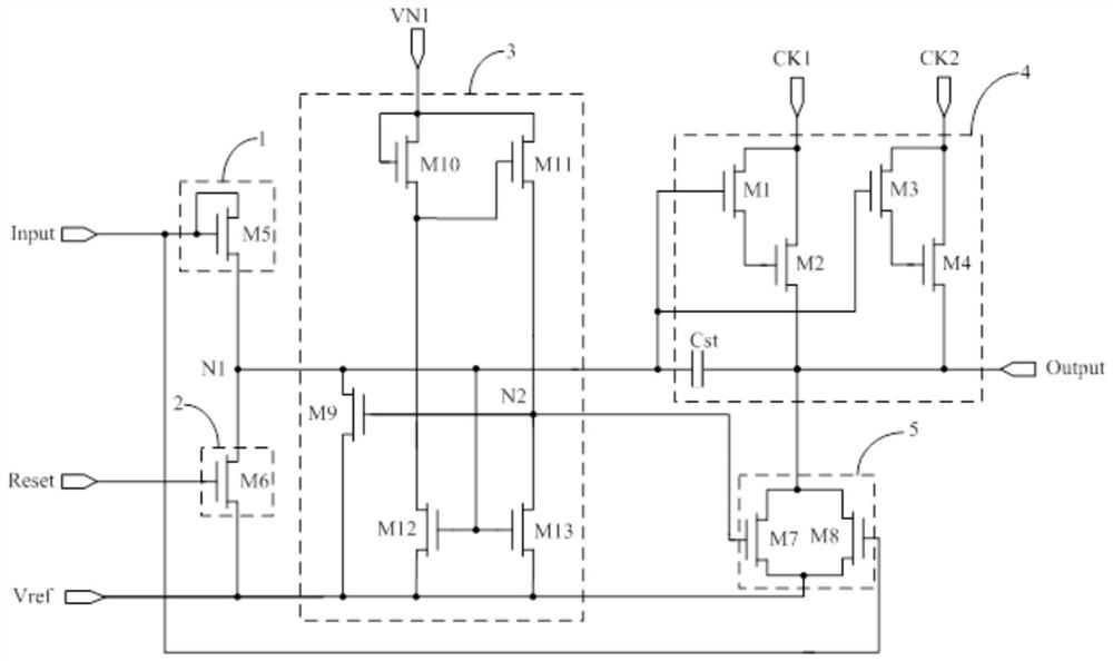
[0124] by Figure 3a Take the shift register shown as an example, all transistors are N-type transistors; the signal of the reference voltage signal terminal Vref is a low potential signal, and the signal of the first node control signal terminal VN1 is a high potential signal; the corresponding input and output timing diagram is as follows Figure 4a shown. Specifically, choose the Figure 4a There are two stages T1 and T2 in the shown input and output timing diagram; wherein, the T1 stage and the T2 stage respectively correspond to 2s in the period of the signal of the first clock signal terminal CK1. In addition, four stages T11, T12, T13 and T14 in the time of displaying one frame in the T1 stage are selected; and four stages T21, T22, T23 and T24 in the time of displaying one frame in the T2 stage are selected.

[0125] In the T11 stage, Input=1, Reset=0, CK1=1, CK2=0. Since Input=1, both the fifth switch transistor M5 and the eighth switch transistor M8 are turned on....

Embodiment 2

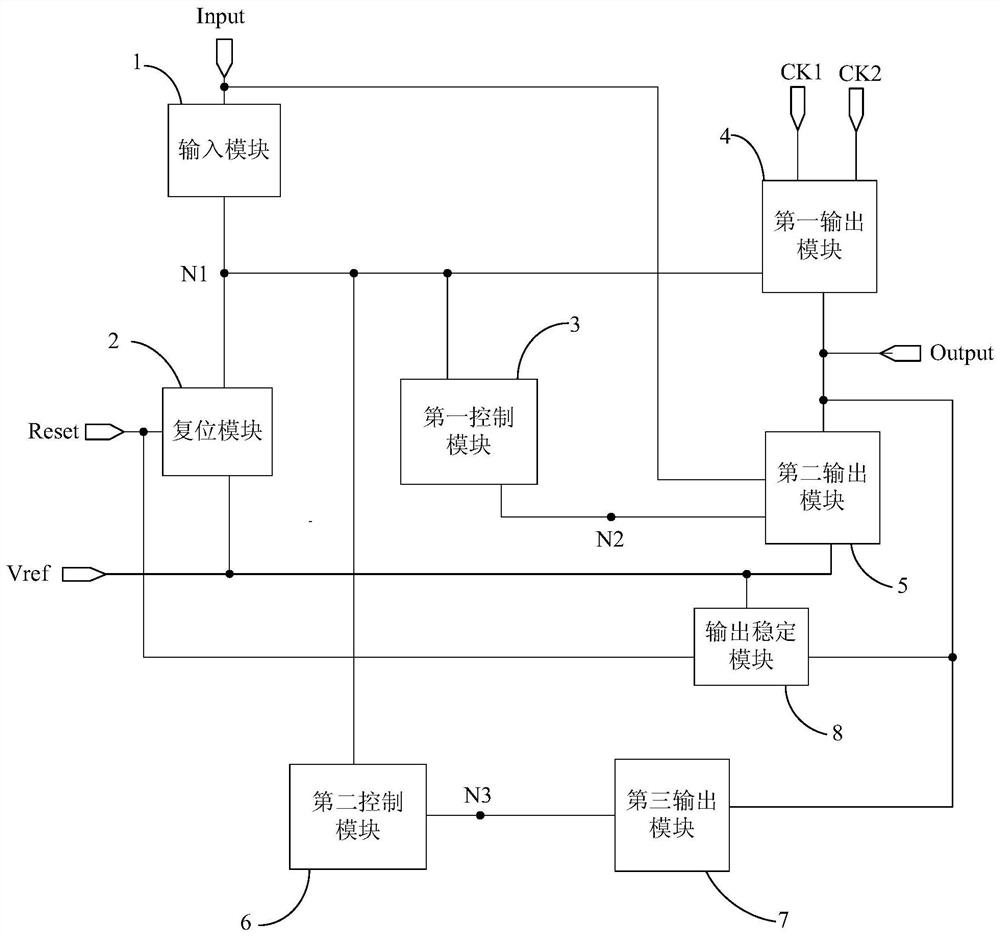
[0137] by Figure 3b Taking the shift register shown as an example, all transistors are N-type transistors; the signal of the reference voltage signal terminal Vref is a low potential signal, the signal of the first node control signal terminal VN1 is the same as the signal of the first clock signal terminal CK1, and the signal of the first node control signal terminal CK1 is the same. The signal of the two-node control signal terminal VN2 is the same as the signal of the second clock signal terminal CK2; the corresponding input and output timing diagram is as follows Figure 4b shown. Specifically, choose the Figure 4b There are two stages T1 and T2 in the shown input and output timing diagram; wherein, the T1 stage and the T2 stage respectively correspond to 2s in the period of the signal of the first clock signal terminal CK1. In addition, four stages T11, T12, T13 and T14 in the time of displaying one frame in the T1 stage are selected; and four stages T21, T22, T23 and...


PUM


Abstract

The invention discloses a shift register, a gate drive circuit and a display device, comprising: an input module, a reset module, a first control module, a first output module and a second output module; wherein, since the first output module has two output paths, one of which is to provide the signal at the first clock signal end to the drive signal output end of the shift register under the common control of the first clock signal end and the signal of the first node, and the other path is to Under the common control of the signal terminal and the signal of the first node, the signal of the second clock signal terminal is provided to the drive signal output terminal, and cooperates with the other four modules to make the two paths work alternately, so as to avoid the current flowing only Through one path, the service life of the shift register can be improved.

Description

technical field [0001] The invention relates to the field of display technology, in particular to a shift register, a gate drive circuit and a display device. Background technique [0002] With the rapid development of display technology, displays show a development trend of high integration and low cost. Among them, the GOA (Gate Driver on Array, array substrate row driving) technology integrates the TFT (Thin Film Transistor, thin film transistor) gate switch circuit on the array substrate of the display panel to form a scan drive for the display panel, thus saving The bonding (Bonding) area of ​​the gate integrated circuit (IC, Integrated Circuit) and the wiring space of the fan-out (Fan-out) area can not only reduce the product cost in terms of material cost and manufacturing process, but also make the display panel Aesthetic design with symmetry on both sides and narrow frame; moreover, this integration process can also save the Bonding process in the direction of the ...

Claims


Application Information

Patent Timeline
Patent Type & Authority Patents(China)
IPC IPC(8): G11C19/28G09G3/20
CPCG11C19/28G09G2310/0267G09G3/3677G09G3/3266G09G2310/0286G09G3/20G09G2310/08G09G2320/043
Inventor 陈康喜汪敏董慧王洪军王建军
Owner BOE TECH GRP CO LTD
Why Eureka
Try Eureka