

Lamination and connection process of wafers in 3d NAND flash memory structure
A wafer and flash memory technology, which is applied in the field of wafer lamination and connection technology, can solve the problems affecting the performance of 3D NAND flash memory structure products, reduce the interface bonding force after lamination and connection, and affect the effect of lamination and connection, etc., to achieve enhanced bonding Combined force, improve product performance, increase the effect of interface bonding force
- Summary
- Abstract
- Description
- Claims
- Application Information
AI Technical Summary
Problems solved by technology
Method used
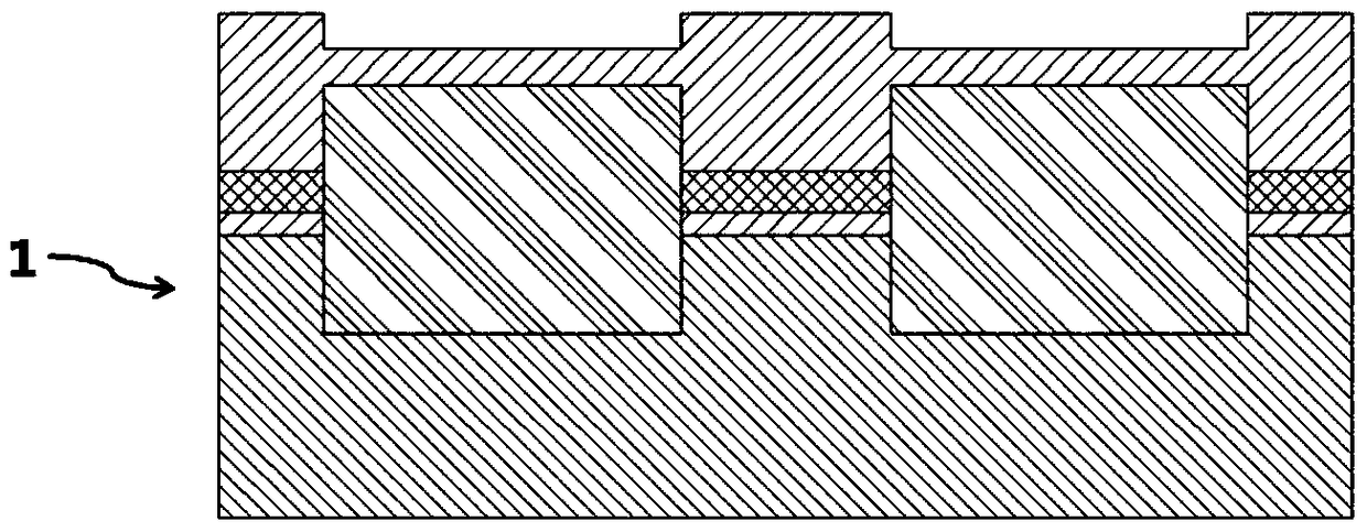
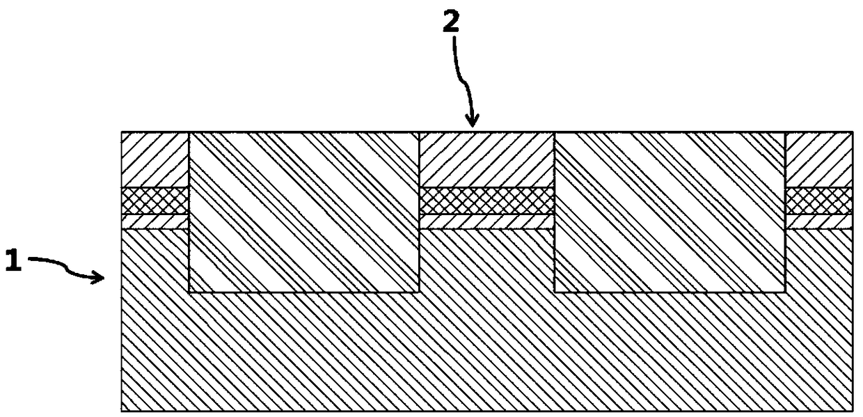
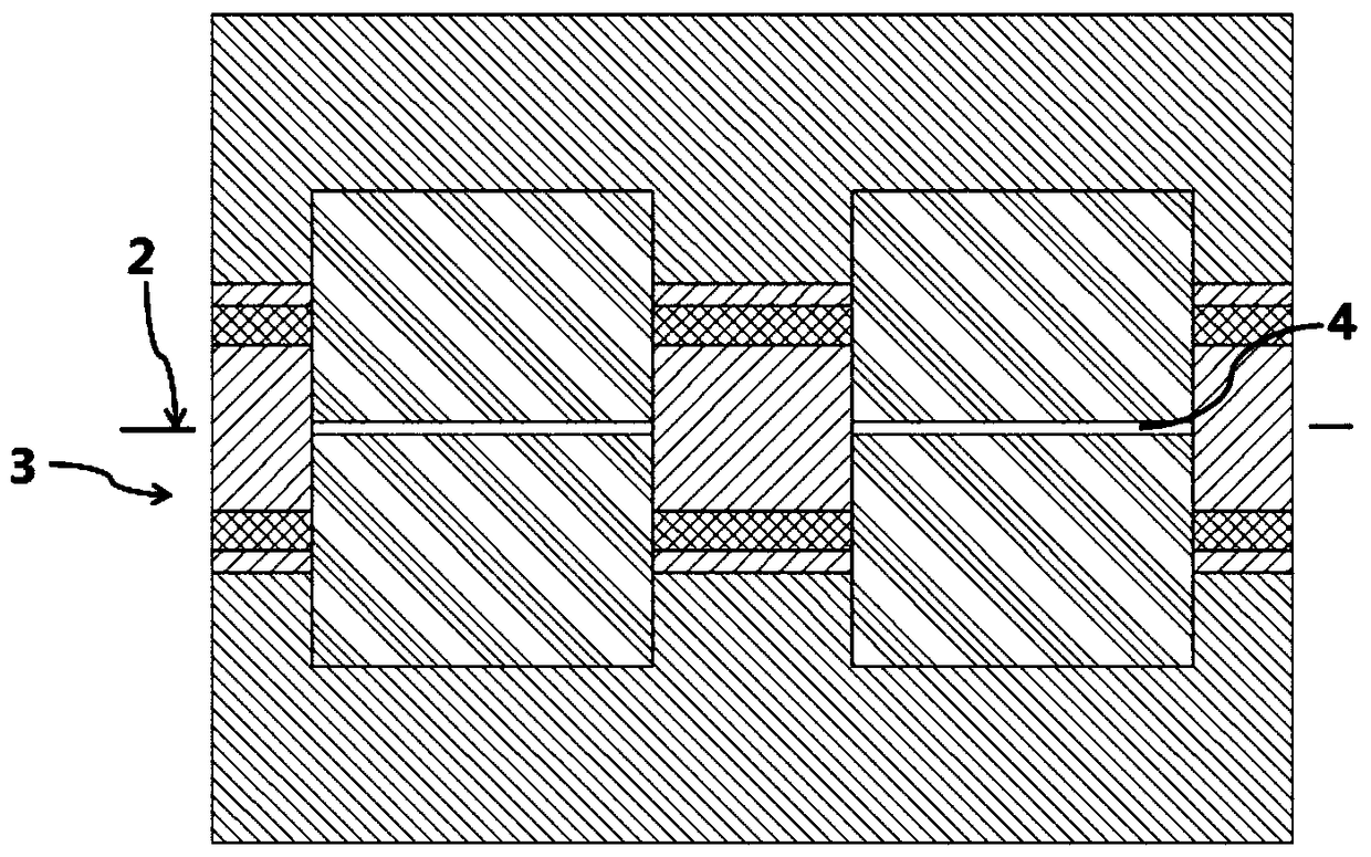
Image

Examples
Embodiment Construction
[0032] Exemplary embodiments of the present disclosure will be described in more detail below with reference to the accompanying drawings. Although exemplary embodiments of the present disclosure are shown in the drawings, it should be understood that the present disclosure may be embodied in various forms and should not be limited by the embodiments set forth herein. Rather, these embodiments are provided for more thorough understanding of the present disclosure and to fully convey the scope of the present disclosure to those skilled in the art.
[0033] In the interest of clarity, not all features of an actual implementation are described. In the following description, well-known functions and constructions are not described in detail since they would obscure the invention with unnecessary detail. It should be appreciated that in the development of any actual embodiment, numerous implementation details must be worked out to achieve the developer's specific goals, such as ch...
PUM
 Abstract
Description
Claims
Application Information