High-frequency multi-layer circuit board hole conduction technology and high-frequency multi-layer circuit board using it

A multi-layer circuit and inner-layer circuit technology, applied in the direction of multi-layer circuit manufacturing, printed circuit components, etc., can solve the problems of high cost, easy peeling of hole copper, complicated process, etc., and achieve high product yield and low cost. Effect

Active Publication Date: 2020-01-07
CHUNHUA TECHNOLOGICAL KUSN
View PDF3 Cites 0 Cited by
  • Summary
  • Abstract
  • Description
  • Claims
  • Application Information

AI Technical Summary

Problems solved by technology

The steps in the dotted line box in this process are all wet process production, so the disadvantages of this existing process are: subject to wet process production, potion ratio, strict testing requirements, high cost of sewage treatment in production, complicated process, impossible Production of multi-layer boards with thick boards and small holes 5 (that is, via holes with small apertures), that is, multi-layer boards with a large aspect ratio (aspect ratio = board thickness / aperture diameter), has poor functions such as broken holes
And the high-frequency material is smooth, there is a risk that the hole copper is easy to peel off
At present, the development of flexible circuit boards tends to be denser and thinner. In the long run, the process of using copper plating in holes is complicated and costly

Method used


Image

  • High-frequency multi-layer circuit board hole conduction technology and high-frequency multi-layer circuit board using it
  • High-frequency multi-layer circuit board hole conduction technology and high-frequency multi-layer circuit board using it
  • High-frequency multi-layer circuit board hole conduction technology and high-frequency multi-layer circuit board using it

Examples


Embodiment 1

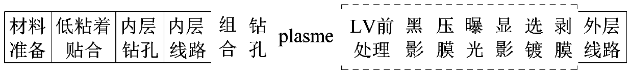
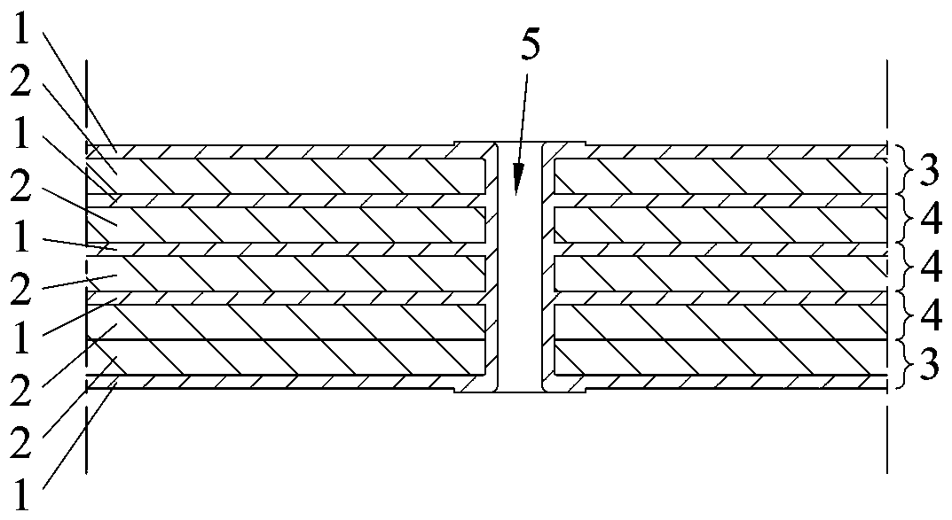
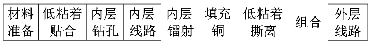
[0031] Example 1: As attached image 3 And Figure 4 As shown, a high-frequency multilayer circuit board hole conduction process for making a high-frequency multilayer circuit board with internal conduction via holes 7 includes the following steps:

[0032] 1. Prepare several inner single-layer boards 4 and two outer single-layer boards 3

[0033] (1) Material preparation, that is, copper foil distribution: prepare the copper foil composed of the base layer 2 and the copper layer 1 on one side of the base layer 2;

[0034] (2) Low-adhesion lamination: lamination of the low-adhesion layer on the other side surface of the base layer 2;

[0035] (3) Inner layer drilling: set positioning holes 6 through the low adhesion layer, base layer 2 and copper layer 1;

[0036] Through the above steps, the prototype of the outer single layer board 3 or the inner single layer board 4 can be obtained. For the inner single-layer board 4, continue to obtain through the following steps:

[0037] (4) Fabri...


PUM


Abstract

The invention relates to a high frequency multilayer circuit board hole conduction technology comprising the steps that multiple internal single-layer boards and two external single-layer boards are prepared, the internal single-layer boards and the external single-layer boards comprise a copper layer, a base layer and a low adhesive layer, the internal single-layer boards and the external single-layer boards are provided with positioning holes through the copper layer, the base layer and the low adhesive layer, and internal lines are formed in the copper layers of the internal single-layer boards; conduction holes are arranged on each internal single-layer board and each external single-layer board by using a laser method so that the conduction holes on the internal single-layer boards are enabled to be connected with the internal lines and the conduction holes on the external single-layer boards are enabled to be connected with the copper layer of the external single-layer boards; copper conductors are filled in the conduction holes so that the copper conductors are enabled to be connected with the internal lines of the internal single-layer boards or the copper layer of the external single-layer boards; and multiple internal single-layer boards and two external single-layer boards are combined and connected and external lines are manufactured on the copper layer of the external single-layer boards so as to form the high frequency multilayer circuit board. Compared with the technologies in the prior art, the high frequency multilayer circuit board hole conduction technology is simple and practicable and low in cost.

Description

Technical field [0001] The invention belongs to the field of circuit board production, and specifically relates to a high-frequency multilayer circuit board hole conduction process and a high-frequency multilayer circuit board product produced by applying the process. Background technique [0002] At present, the high-frequency multilayer circuit board has passed the attached figure 1 The hole shown is through the copper plating process to make through holes for conducting each layer. The products using this process are as attached figure 2 Gesture. The process is mature and is the mainstream production process in the industry. The steps in the dashed box in this process are all wet process production. Therefore, the disadvantages of the existing process are that it is subject to wet process production, the ratio of medicines and water, strict testing requirements, high cost of processing wastewater in production, and complicated processes. The production of multi-layer boards ...

Claims


Application Information

Patent Timeline
Patent Type & Authority Patents(China)
IPC IPC(8): H05K1/02H05K3/46
Inventor 孙承楼翟健康
Owner CHUNHUA TECHNOLOGICAL KUSN
Why Eureka
Try Eureka