
Touch display device and manufacturing method thereof

A technology of a touch display device and a manufacturing method, which is applied in semiconductor/solid-state device manufacturing, instruments, semiconductor devices, etc., to achieve the effects of reducing metallic luster, promoting light scattering, and improving yield

Active Publication Date: 2020-11-17
INTERFACE TECH CHENGDU CO LTD +2
View PDF6 Cites 0 Cited by
  • Summary
  • Abstract
  • Description
  • Claims
  • Application Information

AI Technical Summary

Problems solved by technology

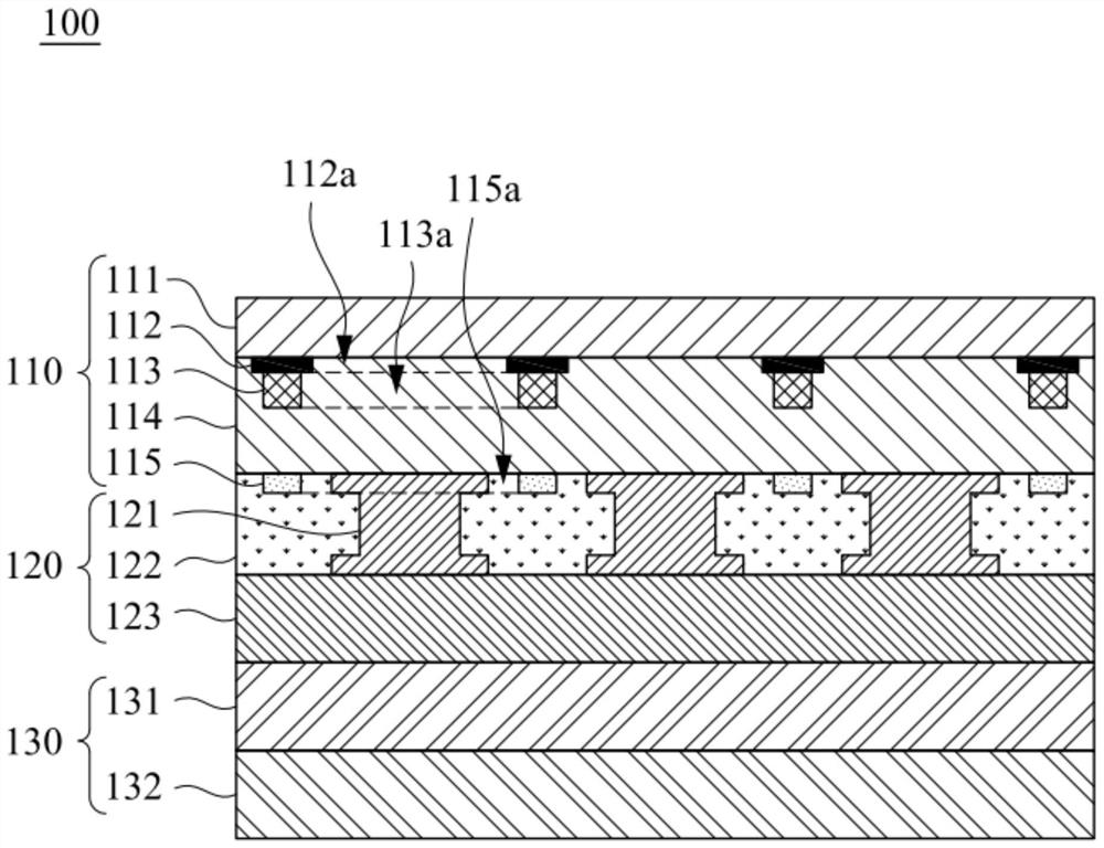
[0003] The technical problem to be solved by the present invention is to provide a touch display device and its manufacturing method, which can reduce the problem that the reflected light of the metal grid layer affects the visual effect

Method used


Image

  • Touch display device and manufacturing method thereof
  • Touch display device and manufacturing method thereof
  • Touch display device and manufacturing method thereof

Examples


Embodiment Construction

[0046] The present invention is further described below.

[0047] Several embodiments of the present invention will be disclosed in the following figures. For the sake of clarity, many practical details will be described together in the following description. It should be understood, however, that these practical details should not be used to limit the invention. That is, in some embodiments of the present invention, these practical details are unnecessary. In addition, for the sake of simplifying the drawings, some commonly used structures and components will be shown in a simple and schematic manner in the drawings. And, unless otherwise indicated, the same component symbols in different drawings can be considered as corresponding components. The illustrations in these drawings are for clearly expressing the connection relationship between the various components in these embodiments, and do not show the actual size of the various components.

[0048] Please refer to figu...


PUM


Abstract

The invention discloses a touch display device, which includes a substrate, a light absorbing layer, a first metal grid layer, an insulating layer and a second metal grid layer. The light absorbing layer is disposed on the substrate. The first metal mesh layer is disposed on the light absorbing layer. The insulating layer is disposed on the substrate and covers the first metal grid layer and the light absorbing layer. The second metal grid layer is located on a side of the insulating layer away from the first metal grid layer. The touch display device disclosed in the present invention uses the light absorbing layer to reduce the problem that the reflected light of the metal grid layer affects the visual effect, and the uneven metal grid layer promotes light scattering, reduces the metallic luster of the touch display device, and further improves Visual effects.

Description

technical field [0001] The invention relates to a touch display device and a manufacturing method thereof. Background technique [0002] At present, the manufacturing process of the metal mesh of the touch display device is complicated, and the manufacturing processes of the display module and the touch module are likely to interfere with each other, resulting in a low yield rate. In addition, the metal grid has reflection problems, which affects the visual effect of the touch display device. Therefore, how to simplify the manufacturing process, improve the yield rate, solve the reflection problem, etc. are important technical issues in this field. Contents of the invention [0003] The technical problem to be solved by the present invention is to provide a touch display device and a manufacturing method thereof, which can reduce the problem that the reflected light of the metal grid layer affects the visual effect. [0004] The invention discloses a touch display device...

Claims


Application Information

Patent Timeline
Patent Type & Authority Patents(China)
IPC IPC(8): H01L27/32H01L21/77G06F3/041
CPCG06F3/0445G06F3/0412G06F2203/04112G06F2203/04103H10K59/40H10K59/87H10K59/1201H10K50/84H10K59/12
Inventor 张志鹏陈俊铭林子祥
Owner INTERFACE TECH CHENGDU CO LTD
Learn More