Shielding gate MOS structure with gradually changing oxide layer
A MOS structure and shielding grid technology, applied in the direction of electrical components, circuits, semiconductor devices, etc., to achieve low on-resistance, cost saving, and improve the effect of device withstand voltage
- Summary
- Abstract
- Description
- Claims
- Application Information
AI Technical Summary
Problems solved by technology
Method used
Image

Examples
Embodiment Construction
[0041] The present invention will be further described below in conjunction with specific embodiments and drawings.
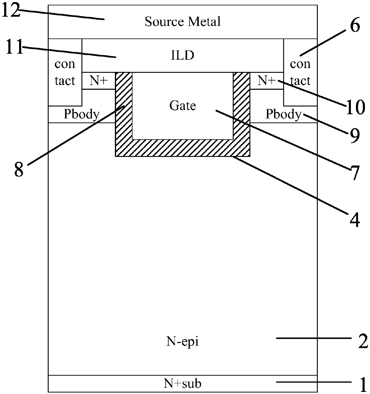
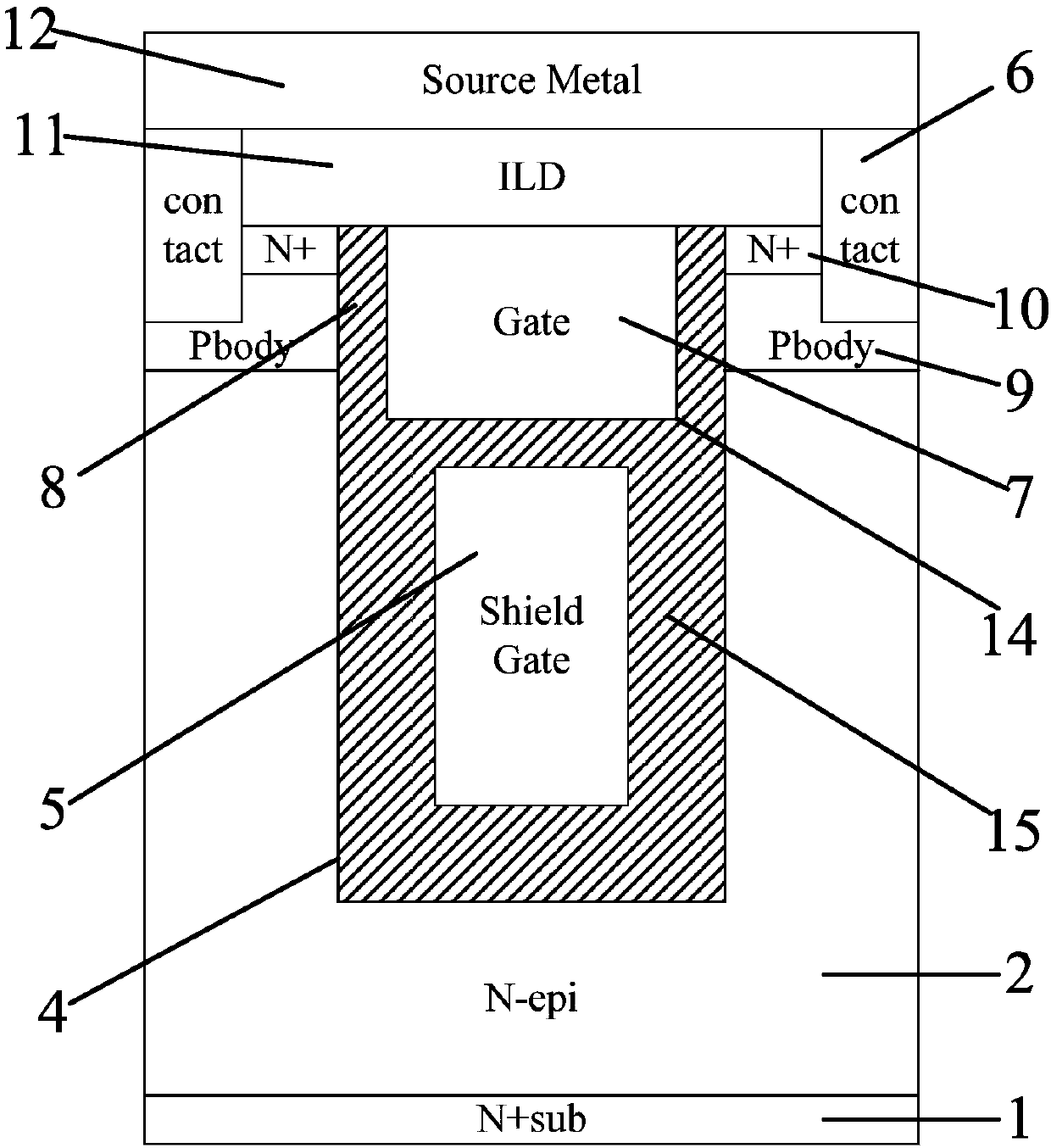
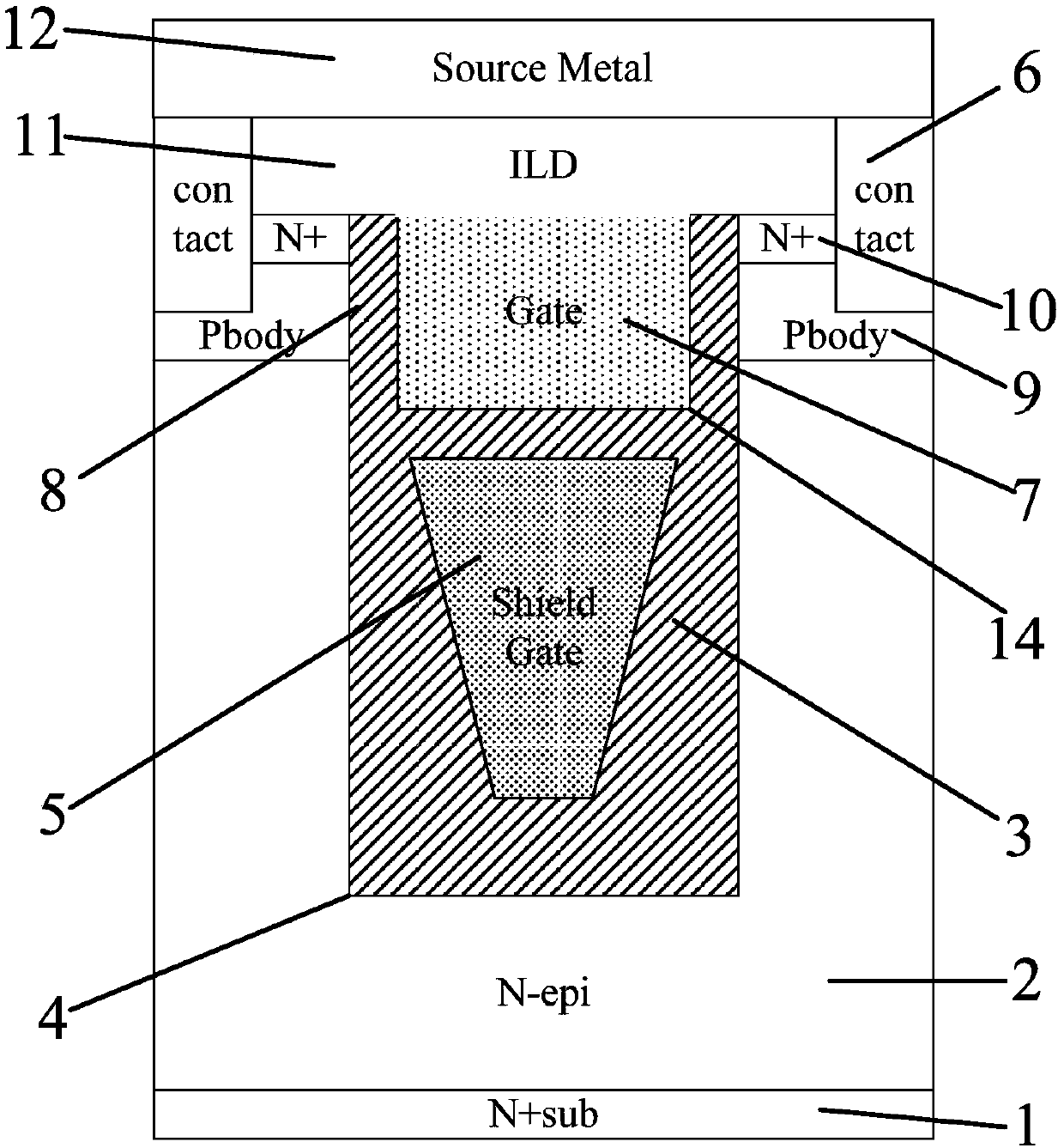
[0042] According to the attached image 3 As described, the shielded gate MOS structure of the embodiment of the present invention takes N-type conductivity as an example. A shielded gate MOS structure with a graded oxide layer includes a cell area and a terminal protection area, and the cell area is located in the central area of the device. The terminal protection area surrounds the cell area, and the cell area is formed by a plurality of MOSFET device unit bodies in parallel, and is characterized in that: the MOSFET device unit body includes a semiconductor substrate, and the semiconductor substrate It includes an N-type heavily doped substrate 1 and an N-type epitaxial layer 2 on the N-type heavily doped substrate 1. The upper surface of the N-type epitaxial layer 2 is the first main surface 001 of the semiconductor substrate. The lower surface of the doped ...
PUM
| Property | Measurement | Unit |
|---|---|---|
| Depth | aaaaa | aaaaa |
Abstract
Description
Claims
Application Information
 - R&D
- Intellectual Property
- Life Sciences
- Materials
- Tech Scout
- Unparalleled Data Quality
- Higher Quality Content
- 60% Fewer Hallucinations
Browse by: Latest US Patents, China's latest patents, Technical Efficacy Thesaurus, Application Domain, Technology Topic, Popular Technical Reports.
© 2025 PatSnap. All rights reserved.Legal|Privacy policy|Modern Slavery Act Transparency Statement|Sitemap|About US| Contact US: help@patsnap.com