Gallium nitride semiconductor device and preparation method therefor

A gallium nitride and semiconductor technology, applied in the fields of semiconductor devices, semiconductor/solid-state device manufacturing, electrical components, etc., can solve the problems of high electric field density, breakdown, leakage of gallium nitride semiconductor devices, etc., to enhance reliability, reduce Small electric field strength, the effect of improving the withstand voltage of the device

Active Publication Date: 2017-10-20
SHENZHEN JING XIANG TECH CO LTD +1
View PDF7 Cites 0 Cited by
  • Summary
  • Abstract
  • Description
  • Claims
  • Application Information

AI Technical Summary

Problems solved by technology

[0004] However, in the prior art, due to the high electric field density, the leakage and breakdown of the GaN semiconductor de

Method used


Image

  • Gallium nitride semiconductor device and preparation method therefor
  • Gallium nitride semiconductor device and preparation method therefor
  • Gallium nitride semiconductor device and preparation method therefor

Examples


Embodiment Construction

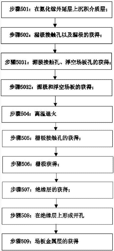
[0037] In order to make the purpose, technical solutions and advantages of the embodiments of the present invention clearer, the technical solutions in the embodiments of the present invention will be clearly and completely described below in conjunction with the drawings in the embodiments of the present invention. Obviously, the described embodiments It is a part of embodiments of the present invention, but not all embodiments. Based on the embodiments of the present invention, all other embodiments obtained by persons of ordinary skill in the art without making creative efforts belong to the protection scope of the present invention.

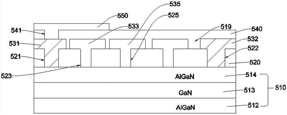
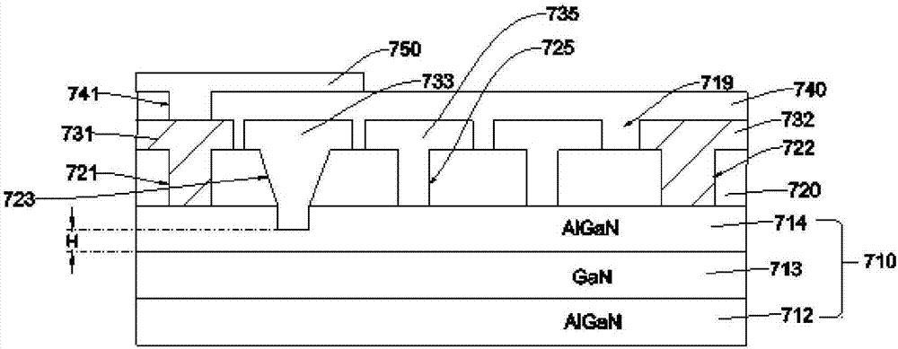
[0038] Please refer to Figure 1a As shown, the embodiment of the present invention provides a gallium nitride semiconductor device, which includes from bottom to top: gallium nitride epitaxial layer 510, dielectric layer 520, source 520 and drain 532, gate 533, insulating layer 540, field Plate metal layer 550 .

[0039] Wherein, the galliu...


PUM

PropertyMeasurementUnit
Thicknessaaaaaaaaaa
Heightaaaaaaaaaa

Abstract

The invention relates to the technical field of semiconductor devices, and provides a gallium nitride semiconductor device. The semiconductor device comprises a gallium nitride epitaxial layer; a dielectric layer which is disposed on the gallium nitride epitaxial layer; a source electrode, a drain electrode and a grid electrode, which are all disposed on the dielectric layer and respectively pass through the dielectric layer to be connected with the gallium nitride epitaxial layer; insulating layers which are disposed on the source electrode, the drain electrode, the grid electrode and the dielectric layer, wherein the insulating layers are made of silicon dioxide. According to the invention, the semiconductor device is not liable to break down an aluminium nitride gallium layer, thereby avoiding the electric leakage and breakdown of the gallium nitride semiconductor device, effectively protecting the gallium nitride semiconductor device, and improving the reliability of the gallium nitride semiconductor device.

Description

technical field [0001] The invention relates to the field of semiconductor technology, in particular to a gallium nitride semiconductor device and a preparation method thereof. Background technique [0002] Gallium nitride has the advantages of large band gap, high electron saturation rate, high breakdown electric field, high thermal conductivity, corrosion resistance and radiation resistance, so gallium nitride can be used to make semiconductor materials to obtain gallium nitride semiconductor devices . [0003] In the prior art, a gallium nitride semiconductor device is prepared by forming a silicon nitride layer on the surface of the gallium nitride epitaxial layer, etching a source contact hole and a drain contact hole on the silicon nitride layer, and Deposit metal in the electrode contact hole and drain contact hole to form the source and drain; then etch the silicon nitride layer and the aluminum gallium nitride layer in the gallium nitride epitaxial layer to form a ...

Claims


Application Information

Patent Timeline
IPC IPC(8): H01L29/06H01L29/40H01L29/423H01L29/47H01L21/335H01L29/778
CPCH01L29/0611H01L29/0638H01L29/402H01L29/42356H01L29/475H01L29/66462H01L29/7783
Inventor 刘美华林信南刘岩军
Owner SHENZHEN JING XIANG TECH CO LTD
Why Eureka
Try Eureka