High-voltage shielding gate MOSFET with floating island structure and manufacturing method

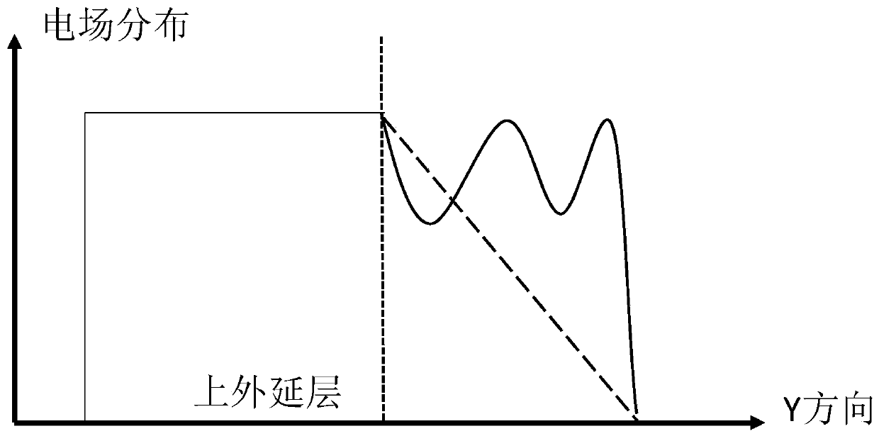
A manufacturing method and technology for shielding gates, which are applied in the manufacture of semiconductor/solid-state devices, electrical components, transistors, etc., can solve problems such as increasing on-resistance, and achieve the effects of reducing on-resistance, improving device withstand voltage, and optimizing electric field distribution.

Pending Publication Date: 2019-11-15
无锡橙芯微电子科技有限公司
View PDF0 Cites 0 Cited by
  • Summary
  • Abstract
  • Description
  • Claims
  • Application Information

AI Technical Summary

Problems solved by technology

[0003] For general low-voltage shielded gate MOSFETs (such as <100V), low-resistance single epitaxy can be directly used to achieve withstand voltage; but for high-voltage shielded gate MOSFETs (such as 100V-300V), double epitaxy is often required to increase the withstand voltage, and the lower epitaxy The resistivity is much higher than that of the upper epitaxy, which will greatly increase the on-resistance
Since the on-resistance and the breakdown voltage are in a contradictory relationship or a compromise relationship, that is, the reduction of the on-resistance is limited by the breakdown voltage, but the means of reducing the on-resistance usually used in the prior art will also limit the endurance Compression capacity

Method used


Image

  • High-voltage shielding gate MOSFET with floating island structure and manufacturing method
  • High-voltage shielding gate MOSFET with floating island structure and manufacturing method

Examples


Embodiment Construction

[0038] In order to make the object, technical solution and advantages of the present invention clearer, the present invention will be described in further detail below in conjunction with specific embodiments and with reference to the accompanying drawings. Wherein the same components are denoted by the same reference numerals. It should be noted that the words "front", "rear", "left", "right", "upper" and "lower" used in the following description refer to directions in the drawings. The terms "inner" and "outer" are used to refer to directions toward or away from, respectively, the geometric center of a particular component.

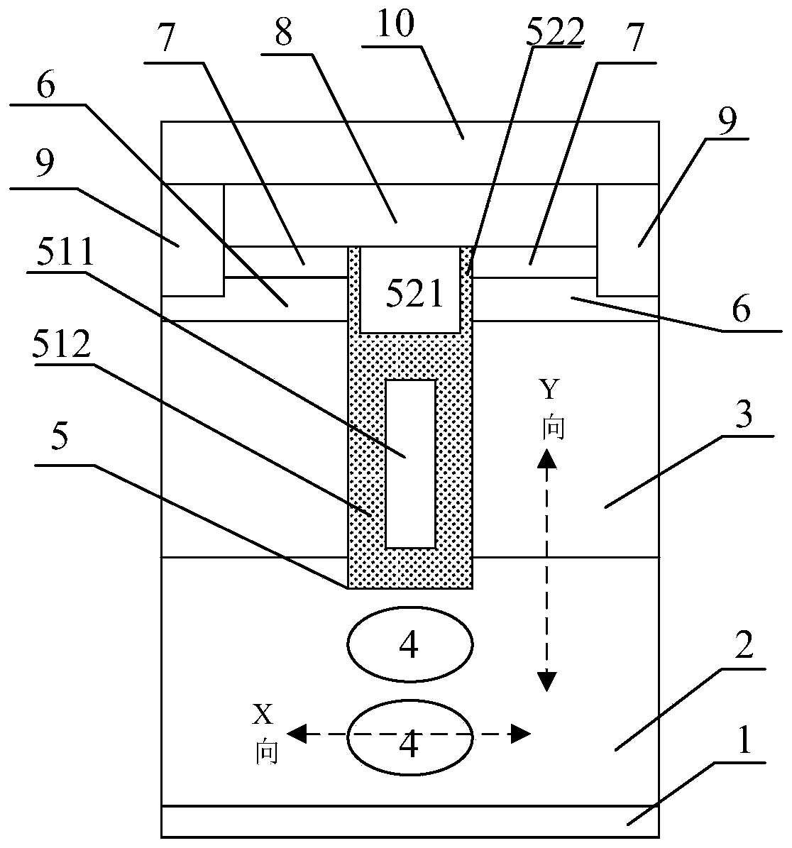
[0039] The existing MOS structure includes a cell area and a terminal protection area, the cell area is located in the central area of ​​the device, the terminal protection area surrounds the cell area, and the cell area is composed of several MOSFET devices The units are connected in parallel.

[0040] As a first aspect of the present invention, a hi...


PUM


Abstract

The invention relates to the technical field of semiconductor device manufacturing, in particular to a high-voltage shielding gate MOSFET with a floating island structure and a manufacturing method. The high-voltage shielding gate MOSFET with a floating island structure includes a semiconductor substrate. The semiconductor substrate includes an N-type substrate and an epitaxial layer growing on the N-type substrate. The epitaxial layer includes a lower epitaxial layer and an upper epitaxial layer growing on the lower epitaxial layer. The lower epitaxial layer is provided with a P-type floatingisland region. The upper epitaxial layer is provided with a groove which extends from a first main surface to a second main surface. The upper part of the groove is a gate region, the lower part of the grove is a shielding gate region, and the gate region and the shielding gate region are isolated by an oxide layer. The gate region is provided with a gate layer and a gate oxide layer. The shielding gate region is provided with a shielding gate layer and a shielding gate oxide layer. High withstand voltage can be achieved, and the on resistance can be greatly reduced because of the adoption ofthe low-resistance lower epitaxial layer.

Description

technical field [0001] The invention relates to the technical field of manufacturing semiconductor devices, in particular to a high-voltage shielded gate MOSFET with a floating island structure and a manufacturing method. Background technique [0002] Shielded gate MOS is based on traditional trench gate MOS, using thick oxide layer and discrete shielded gate to achieve lateral auxiliary depletion, so that lower resistance epitaxy can be used to achieve high withstand voltage requirements and reduce on-resistance. [0003] For general low-voltage shielded gate MOSFETs (such as <100V), low-resistance single epitaxy can be directly used to achieve withstand voltage; but for high-voltage shielded gate MOSFETs (such as 100V-300V), double epitaxy is often required to increase the withstand voltage, and the lower epitaxy The resistivity is much higher than that of the upper epitaxy, which will greatly increase the on-resistance. Since the on-resistance and the breakdown voltag...

Claims


Application Information

Patent Timeline
IPC IPC(8): H01L29/786H01L29/423H01L29/06H01L23/552H01L21/336
CPCH01L29/78642H01L29/0611H01L29/4236H01L29/66742H01L23/552
Inventor 钱振华张艳旺
Owner 无锡橙芯微电子科技有限公司
Why Eureka
Try Eureka