Diamond inclined mesa heterojunction diode and preparation method thereof
A diamond and heterojunction technology, applied in semiconductor/solid-state device manufacturing, electrical components, circuits, etc., can solve the problems of insufficient activation of dopants, difficult growth of n-type diamond, and lack of efficient terminal structure of JBS/MPS structure devices System research and other issues to achieve the effect of alleviating the concentration of fringe electric field, improving the withstand voltage of the device, and good reverse off-state characteristics
- Summary
- Abstract
- Description
- Claims
- Application Information
AI Technical Summary
Problems solved by technology
Method used
Image

Examples
Embodiment 1
[0046] A diamond inclined mesa heterojunction diode structure of the present invention is as follows Figure 7 As shown, its structure includes ohmic contact electrode (7), low-resistance p-type diamond substrate (1), p-type diamond transition layer (2), diamond drift layer (3), and inclined mesa (4) from bottom to top. , groove structure (5), n-type gallium oxide layer (6), Schottky contact electrode (8).
[0047] The low-resistance p-type diamond substrate (1) is single crystal diamond or polycrystalline diamond, and the boron doping concentration is about 10 20 cm -3 .
[0048] The p-type diamond transition layer (2) can be a single-layer or multi-layer boron-doped diamond epitaxial layer, with a thickness of 10 nm to 50 μm, and a boron doping concentration of 10 15 ~10 20 cm -3 Adjust between ranges.
[0049] The diamond drift layer (3) can be a single-layer or multi-layer unintentionally doped diamond epitaxial layer, with a thickness of 10nm to 50μm, and a boron dopi...
Embodiment 2
[0053] The schematic diagram of the preparation method of a diamond inclined mesa heterojunction diode of the present invention is as follows Figure 1-7 shown, including the following steps:
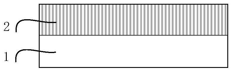
[0054] S1, growing a p-type diamond transition layer (2) on a low-resistance p-type diamond single crystal substrate (1); figure 1 shown.
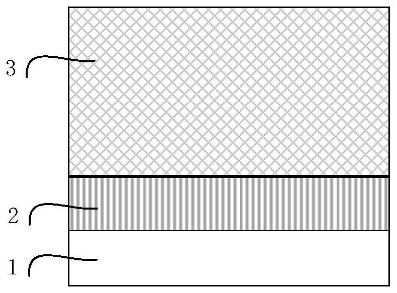
[0055] S2, grow unintentionally doped diamond drift layer (3) on p-type diamond transition layer (2); as figure 2 shown.
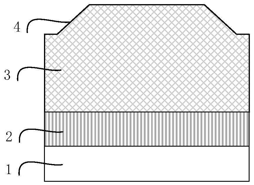
[0056] S3, using photoresist reflow etching on the surface of the diamond drift layer (3) to form an inclined mesa (4); as image 3 shown.
[0057] S4, utilizing oxygen plasma etching to form groove structure (5); Figure 4 shown.
[0058] S5, deposit and form an n-type gallium oxide layer (6) in the inclined mesa (4) and the groove structure (5); as Figure 5 shown.
[0059] S6, form the ohmic contact electrode (7) on the back side of the low-resistance p-type diamond single crystal substrate (1); as Figure 6 shown. ...
PUM
| Property | Measurement | Unit |
|---|---|---|
| Thickness | aaaaa | aaaaa |
Abstract
Description
Claims
Application Information
 - R&D
- Intellectual Property
- Life Sciences
- Materials
- Tech Scout
- Unparalleled Data Quality
- Higher Quality Content
- 60% Fewer Hallucinations
Browse by: Latest US Patents, China's latest patents, Technical Efficacy Thesaurus, Application Domain, Technology Topic, Popular Technical Reports.
© 2025 PatSnap. All rights reserved.Legal|Privacy policy|Modern Slavery Act Transparency Statement|Sitemap|About US| Contact US: help@patsnap.com