OLED display panel encapsulation method and encapsulation structure

A display panel and packaging method technology, which is applied in the manufacture of electrical components, electrical solid devices, semiconductor/solid devices, etc., can solve the problems of complex process, high cost, poor particles and holes, etc., and achieve complex process and good product quality. rate-enhancing effect

Inactive Publication Date: 2018-01-30
WUHAN CHINA STAR OPTOELECTRONICS SEMICON DISPLAY TECH CO LTD
View PDF7 Cites 20 Cited by
  • Summary
  • Abstract
  • Description
  • Claims
  • Application Information

AI Technical Summary

Problems solved by technology

[0006] The object of the present invention is to provide a method for encapsulating OLED display panels, which can effectively solve the complex process existing in the existing OLED thin film encapsulation process, the defects of particles and holes caused by the use of mask plates in the production process, and the cost increase and low temperature. Technical problems such as low film quality and compactness caused by film formation
[0007] Another object of the present invention is to provide a packaging structure for OLED display panels, which can effectively solve the complex process existing in the existing OLED thin-film packaging process, the use of a mask plate in the production process to cause defects such as particles and holes, and increase the cost. , Technical problems such as low film quality and compactness caused by low temperature film formation

Method used


Image

  • OLED display panel encapsulation method and encapsulation structure
  • OLED display panel encapsulation method and encapsulation structure
  • OLED display panel encapsulation method and encapsulation structure

Examples


Embodiment Construction

[0040] In order to further illustrate the technical means adopted by the present invention and its effects, the following describes in detail in conjunction with preferred embodiments of the present invention and accompanying drawings.

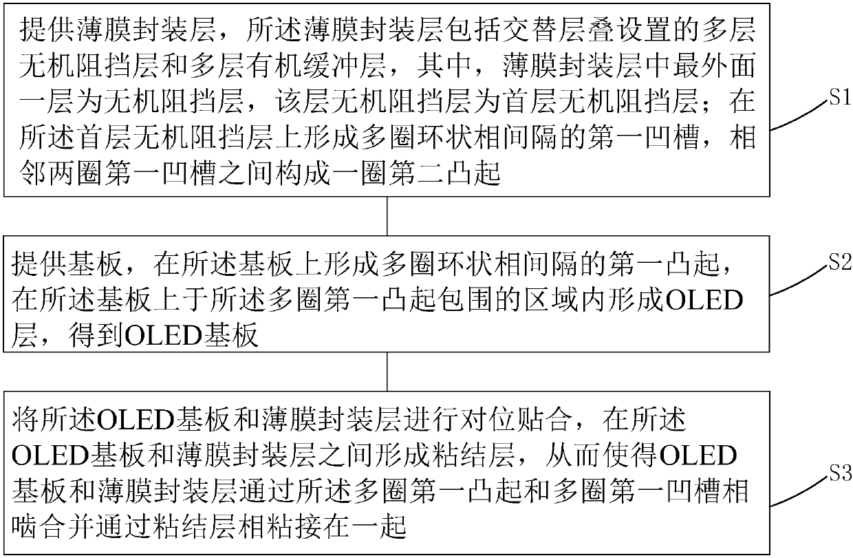
[0041] see figure 1 , the present invention firstly provides a method for encapsulating an OLED display panel, comprising the following steps:

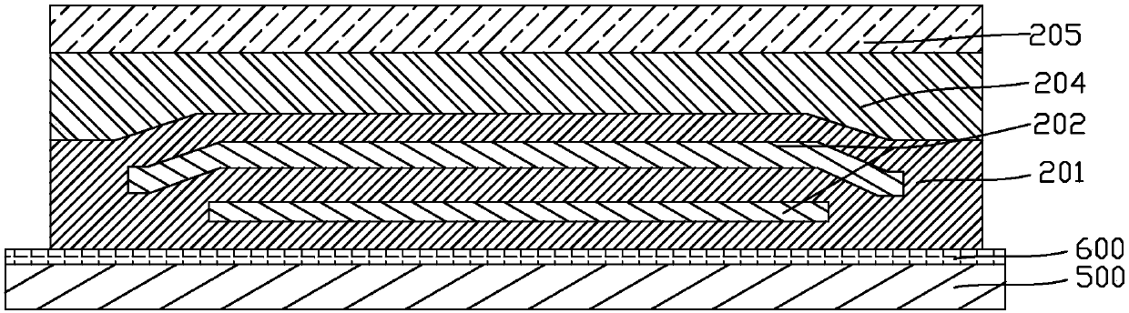
[0042] Step S1, such as Figure 2-6 As shown, a plastic substrate 500 is provided, coated and cured on the substrate 500 to form a layer of optical adhesive layer 600, the cured optical adhesive layer 600 can be peeled off from the substrate 500, and then on the optical adhesive A thin-film encapsulation layer 200 is fabricated on the layer 600, and the thin-film encapsulation layer 200 includes a multi-layer inorganic barrier layer 201 and a multi-layer organic buffer layer 202, wherein the inorganic barrier layer 201 and the organic buffer layer 202 are stacked alternately, and the manufactured Th...


PUM

PropertyMeasurementUnit
thicknessaaaaaaaaaa
thicknessaaaaaaaaaa
thicknessaaaaaaaaaa

Abstract

The invention provides an OLED display panel encapsulation method and encapsulation structure. According to the OLED display panel encapsulation method provided by the invention, a film encapsulationlayer for water and oxygen barrier is independently fabricated with respect to an OLED substrate; a number of annular first grooves and a number of annular first protrusions are formed on the first inorganic barrier layer of the film encapsulation layer and the OLED substrate through photolithography; and a vacuum bonding method is used to bond the OLED substrate and the film encapsulation layer through meshing of a number of first protrusions and a number of first grooves and an adhesive layer, so as to realize the functions of film encapsulation and flexible display. The technical problem that the existing OLED film encapsulation process is complex is effectively solved. Particles, holes and other badness caused by a diaphragm plate and increased cost in the production process are prevented. Low membranous density caused by low temperature film formation and other technical problems are solved. The film encapsulation layer and the OLED substrate are manufactured independently, whichis beneficial to improving the product yield.

Description

technical field [0001] The invention relates to the field of flat panel display technology, in particular to a packaging method and a packaging structure of an OLED display panel. Background technique [0002] Organic Light-Emitting Diode (OLED) displays have the characteristics of self-illumination, high brightness, wide viewing angle, high contrast, flexibility, and low energy consumption. Has begun to gradually replace the traditional liquid crystal display. At present, the application of OLED display panels has become a high-end symbol from small-sized mobile phone display screens to large-sized high-resolution flat-panel TVs. [0003] Unlike traditional liquid crystal display technology, OLED display technology does not require a backlight, and uses very thin coatings of organic materials and glass substrates that emit light when an electric current passes through them. However, because organic materials are easy to react with water vapor or oxygen, as a display devic...

Claims


Application Information

Patent Timeline
Patent Type & Authority Applications(China)
IPC IPC(8): H01L51/52H01L51/56H01L27/32
Inventor 夏存军
Owner WUHAN CHINA STAR OPTOELECTRONICS SEMICON DISPLAY TECH CO LTD
Why Eureka
Try Eureka