2-bite, programmable and digital artificial electromagnetic metasurface
An artificial electromagnetic and metasurface technology, applied in the direction of electrical components, antennas, etc., can solve the problems of reducing the radar scattering cross section, low ability, and inability to achieve anisotropic reflection, etc., to improve the ability to manipulate electromagnetic waves, flexible control, simple and intuitive design Effect
- Summary
- Abstract
- Description
- Claims
- Application Information
AI Technical Summary
Problems solved by technology
Method used
Image
Examples
Embodiment 1
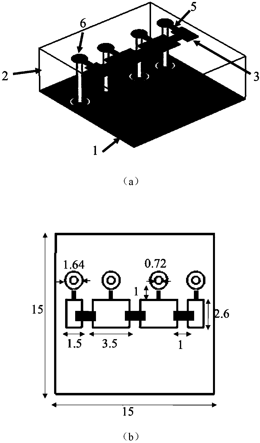
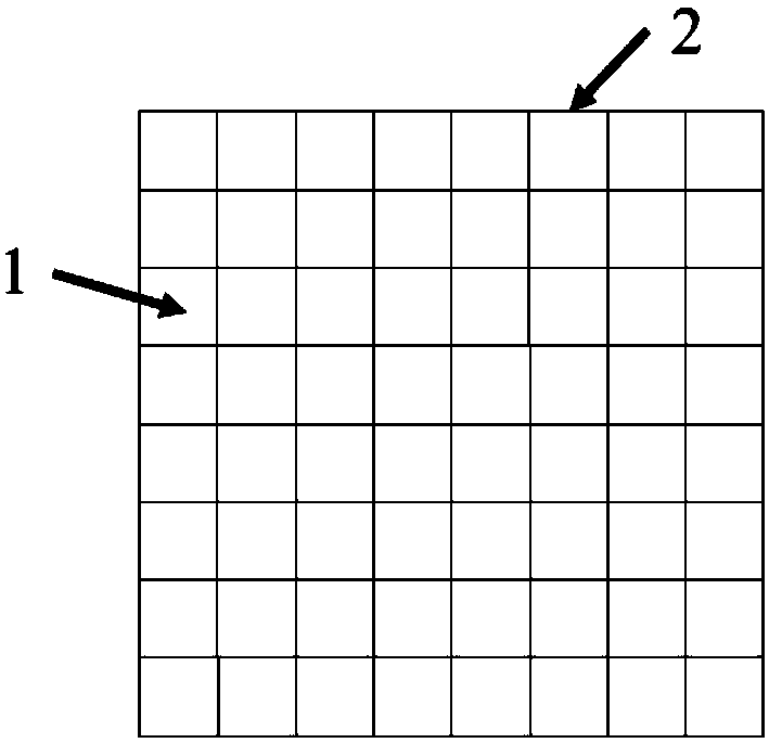
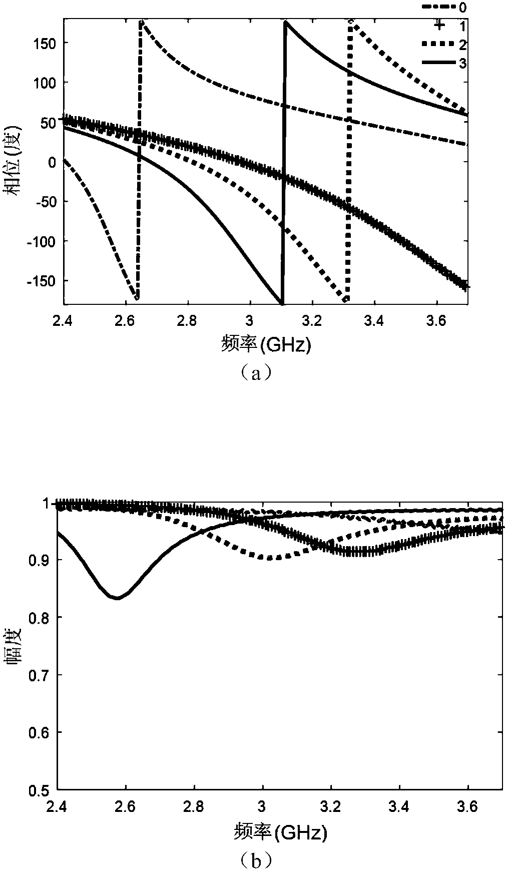
[0023] Such as figure 1 As shown in (a), an artificial electromagnetic metasurface unit of the present embodiment includes: a grounded metal plate 1, a dielectric substrate 2, four metal resonant elements 3, three PIN diodes 4, four metal pads 6 and a choke Inductance 5; wherein, a dielectric substrate is placed on the upper surface of the ground metal plate; four metal resonant elements are engraved on the upper surface of the dielectric substrate; each metal resonant element is connected to the metal pad through a choke inductor; each adjacent A PIN diode is connected across two metal resonant elements; a metal pad in the middle is connected to the ground metal plate through a blind hole; the other metal pads are connected to the bottom three of the dielectric substrate through through holes and isolated from the metal ground plate The metal pads on the bottom three metal pads and the ground metal plate are respectively soldered with wires to connect to the microcontroller o...
Embodiment 2
[0032] Such as Figure 7 As shown in (a), an artificial electromagnetic metasurface unit of the present embodiment includes: ground metal plate 1, dielectric substrate 2, four metal resonant elements 3, five PIN diodes 4, four metal pads 6 and choke Inductance 5; wherein, a dielectric substrate is placed on the upper surface of the grounded metal plate; four metal resonant elements are engraved on the upper surface of the dielectric substrate; each metal resonant element is connected to the metal pad through a choke inductor; the middle two metal A PIN diode is connected across the resonant element, and two PIN diodes are connected between two adjacent metal resonant elements on both sides, so the switching states of the two PIN diodes are the same; a metal pad in the middle passes through Blind holes are connected to the ground metal plate; other metal pads are connected to the three metal pads isolated from the metal ground plate at the bottom of the dielectric substrate thr...
PUM
 Abstract
Description
Claims
Application Information
 - R&D
- Intellectual Property
- Life Sciences
- Materials
- Tech Scout
- Unparalleled Data Quality
- Higher Quality Content
- 60% Fewer Hallucinations
Browse by: Latest US Patents, China's latest patents, Technical Efficacy Thesaurus, Application Domain, Technology Topic, Popular Technical Reports.
© 2025 PatSnap. All rights reserved.Legal|Privacy policy|Modern Slavery Act Transparency Statement|Sitemap|About US| Contact US: help@patsnap.com


