Pixel circuit, driving method thereof, OLED display panel, and display device

A pixel circuit and lighting control technology, applied to static indicators, instruments, etc., can solve the problems of data signal range limitation, limited use scenarios of OLED display panels, and limited brightness adjustment range, etc.

Active Publication Date: 2018-02-09
BOE TECH GRP CO LTD
View PDF9 Cites 7 Cited by
  • Summary
  • Abstract
  • Description
  • Claims
  • Application Information

AI Technical Summary

Problems solved by technology

[0003] In the OLED display panel, due to the limitation of the manufacturing process, the range of the data signal transmitted to the pixel will be limited, so that the brightness adjustment range is limited.
The limited brightness adjustment range will further limit the usage scenarios of OLED display panels

Method used


Image

  • Pixel circuit, driving method thereof, OLED display panel, and display device
  • Pixel circuit, driving method thereof, OLED display panel, and display device
  • Pixel circuit, driving method thereof, OLED display panel, and display device

Examples


Embodiment 1

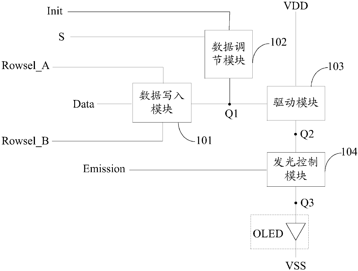
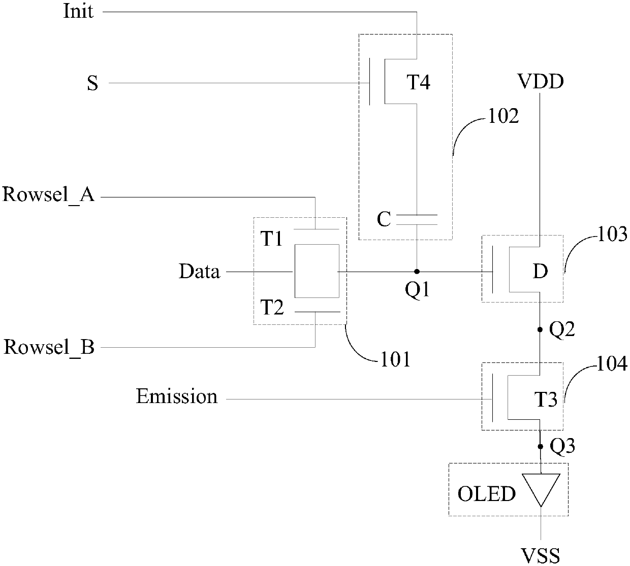
[0080] figure 2 It is a schematic structural diagram of a pixel circuit provided by Embodiment 1 of the present invention. exist figure 2 In the pixel circuit shown, the first switching transistor T1, the third switching transistor T3 and the fourth switching transistor T4 are all N-type transistors, and the second switching transistor T2 and the driving transistor D are all P-type transistors; The transistors are turned on under the action of the high level, and are turned off under the action of the low level; each P-type transistor is turned on under the action of the low level, and is turned off under the action of the high level. The working timing diagram corresponding to the pixel circuit is Image 6 Shown, specifically, choose Image 6 The data writing phase t1, the data range adjustment phase t2, and the light emitting phase t3 in the shown working sequence diagram are described in detail as examples.

[0081] Data writing stage t1: the voltage control signal te...

Embodiment 2

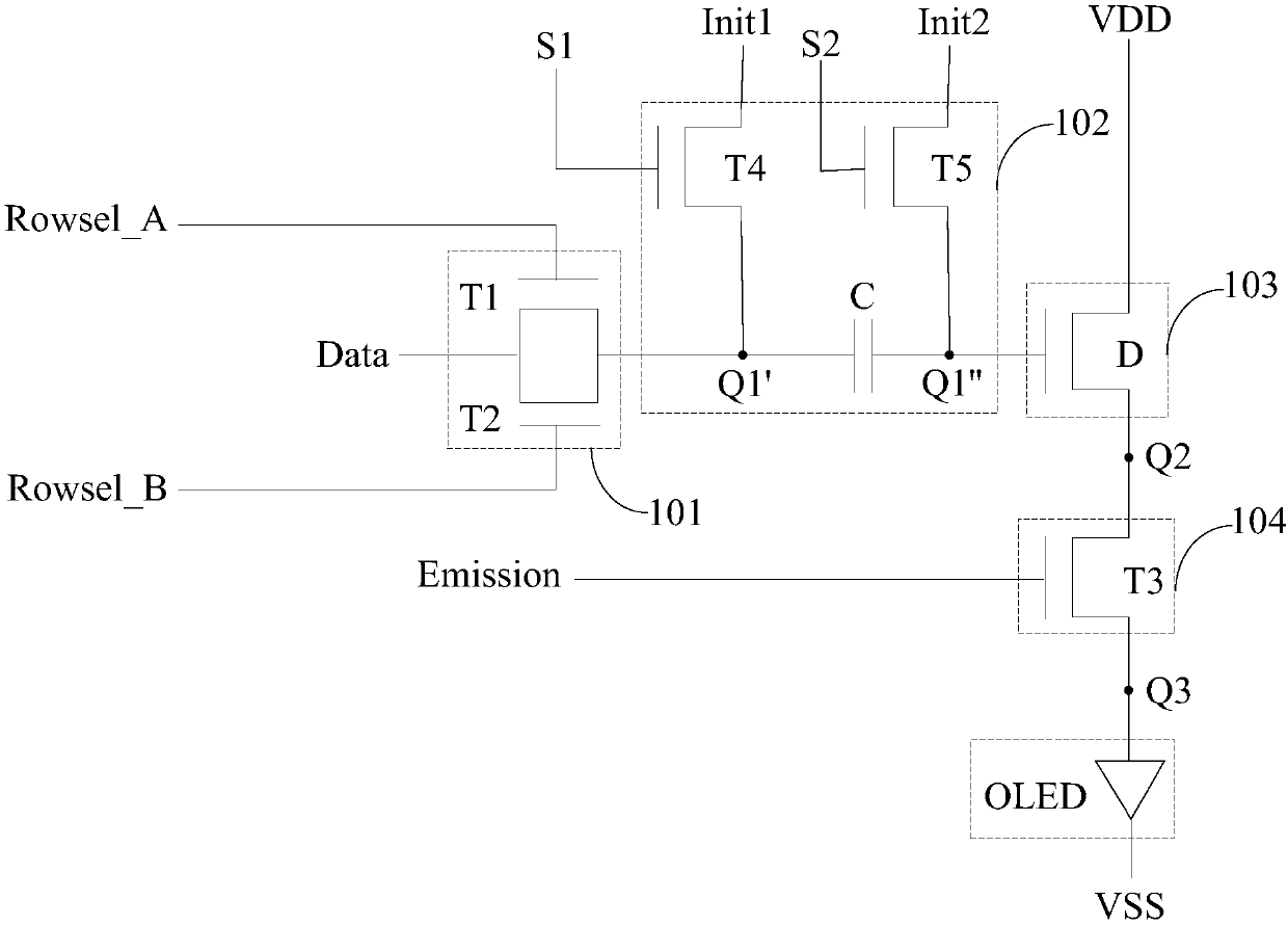
[0092] image 3 It is a schematic structural diagram of the pixel circuit provided by Embodiment 2 of the present invention. exist image 3 In the pixel circuit shown, the first switching transistor T1, the third switching transistor T3, the fourth switching transistor T4 and the fifth switching transistor T5 are all N-type transistors, and the second switching transistor T2 and the driving transistor D are all P-type transistors ; Wherein, each N-type transistor is turned on under the action of high level, and is turned off under the action of low level; each P-type transistor is turned on under the action of low level, and is turned off under the action of high level. The working timing diagram corresponding to the pixel circuit is Figure 7 Shown, specifically, choose Figure 7 The initialization phase t1, the data range adjustment phase t2, and the lighting phase t3 in the shown working sequence diagram are taken as examples for detailed description.

[0093] Initializ...


PUM


Abstract

The invention discloses a pixel circuit, a driving method thereof, an OLED display panel, and a display device; the pixel circuit comprises a data write-in module, a data adjusting module, a drive module, a lighting control module and a lighting device; the data write-in module and the data adjusting module provide data signals and signal variation of an initialized signal end to a control end ofthe drive module, wherein the signal variation of the initialized signal end is >0 and smaller than or equal to the data signal variation of the data signal end, thus enabling the drive module controlend to not only receive the data signal but also receive the signal variation of an initialized signal end, increasing the drive module control end voltage change range, further improving the lighting device brightness adjusting scope, and enlarging the application scene scope.

Description

technical field [0001] The invention relates to the field of display technology, in particular to a pixel circuit, a driving method thereof, an organic light-emitting display panel, and a display device. Background technique [0002] With the popularization of the Internet and the continuous development of display technology, high-quality display panels have become an important feature of many electronic consumer products. Compared with Liquid Crystal Display (LCD), Organic Light Emitting Diode (OLED) has the advantages of self-illumination, low energy consumption, low production cost, wide viewing angle, high contrast, fast response, The color display is more realistic, and it is easier to realize the advantages of thinness, lightness and flexibility. At present, OLED display panels have begun to replace traditional LCD display panels in display fields such as mobile phones, digital cameras, computers, and personal digital assistants, and are expected to become the mainstr...

Claims


Application Information

Patent Timeline
Patent Type & Authority Applications(China)
IPC IPC(8): G09G3/3275G09G3/3291
CPCG09G3/3275G09G3/3291
Inventor 岳晗陈小川玄明花杨盛际卢鹏程王磊张粲王灿杨明刘冬妮
Owner BOE TECH GRP CO LTD
Why Eureka
Try Eureka