Manufacturing method of target assembly

A manufacturing method and component technology, applied in manufacturing tools, metal processing equipment, welding equipment, etc., can solve problems such as low yield, and achieve the effects of improving yield, easy plastic deformation, and reducing fragmentation.

Active Publication Date: 2020-04-28
KONFOONG MATERIALS INTERNATIONAL CO LTD
View PDF5 Cites 0 Cited by
  • Summary
  • Abstract
  • Description
  • Claims
  • Application Information

AI Technical Summary

Problems solved by technology

[0006] However, the yield rate of silicon carbide target assembly formed in the prior art is low

Method used


Image

  • Manufacturing method of target assembly
  • Manufacturing method of target assembly
  • Manufacturing method of target assembly

Examples


Embodiment Construction

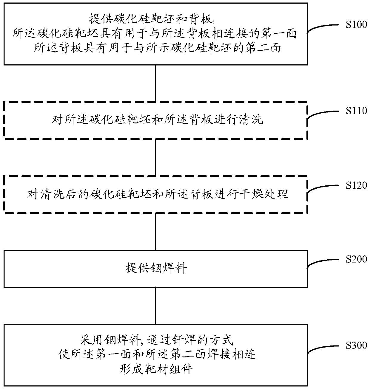
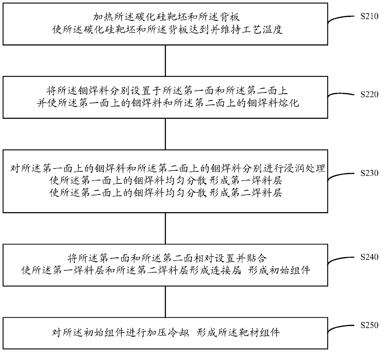
[0035] It can be seen from the background art that the silicon carbide target assembly in the prior art has the problem of low yield. Now combined with the structure of the silicon carbide target component to analyze the reasons for its low yield:

[0036] The silicon carbide target assembly is formed by welding the silicon carbide target blank and the back plate by using solder. In the prior art, the method of manufacturing silicon carbide target components usually uses tin solder to realize the welding of the two.

[0037] Silicon carbide material is relatively brittle, and it is prone to cracking during the manufacturing process of target components. Moreover, tin solder has high hardness after cooling and solidification, and it is difficult to play a buffering role between the silicon carbide target blank and the back plate. Therefore, in the prior art, tin solder is used to connect the silicon carbide target blank and the back plate by welding. SiC target blanks are pro...


PUM

PropertyMeasurementUnit
thicknessaaaaaaaaaa
sizeaaaaaaaaaa

Abstract

The invention discloses a manufacturing method of a target material assembly. The manufacturing method comprises the steps that a silicon carbide target billet and a backboard are provided, wherein the silicon carbide target billet is provided with a first surface connected with the backboard, and the backboard is provided with a second surface connected with the silicon carbide target billet; indium solder is provided; and the indium solder is adopted, and the first surface and the second surface are welded through braze welding. In the technical scheme, the silicon carbide target billet andthe backboard are welded through the indium solder, and the target material assembly is formed; and compared with solder adopted in the prior art, the indium solder has the advantages that after cooling solidification, hardness is relatively small, the indium solder is liable to perform plastic deformation and has a certain buffer function between the silicon carbide target billet and the backboard, the phenomenon that the silicon carbide target billet breaks is reduced, the yield for manufacturing the silicon carbide target material assemblies is increased, and the welding binding rate between the silicon carbide target billet and the backboard is larger than 95%.

Description

technical field [0001] The invention relates to the field of target material manufacturing, in particular to a manufacturing method of a target material component. Background technique [0002] Magnetron sputtering is a coating process that uses charged particles to bombard the target, causing the target atoms to overflow from the surface and evenly deposit on the substrate. Magnetron sputtering has the advantages of high sputtering rate, low substrate temperature, good bonding force between substrate and film, and excellent film uniformity. Magnetron sputtering technology has been widely used in the manufacturing process of electronic and information industries such as integrated circuits, information storage devices, liquid crystal displays, laser memories, and electronic control devices. [0003] With the rapid development of the electronics industry, for example, in the manufacturing process of integrated circuits, the size of chip substrates continues to increase, whil...

Claims


Application Information

Patent Timeline
Patent Type & Authority Patents(China)
IPC IPC(8): B23K1/00B23K1/19B23K1/20
CPCB23K1/0008B23K1/19B23K1/20
Inventor 姚力军潘杰相原俊夫王学泽段高林
Owner KONFOONG MATERIALS INTERNATIONAL CO LTD
Why Eureka
Try Eureka