Method and device of FPGA (Field-Programmable Gate Array) prototype verification on chip

A prototype verification, chip technology, applied in the field of electronics, can solve problems such as inability to verify digital circuits

Inactive Publication Date: 2018-03-06
HISENSE VISUAL TECH CO LTD
View PDF6 Cites 3 Cited by
  • Summary
  • Abstract
  • Description
  • Claims
  • Application Information

AI Technical Summary

Problems solved by technology

Moreover, FPGA prototype verification has a good match for the basic logic design in ordinary digital circuits, but FPGA prototype verification cannot perform good verification on digital circuits that require low power consumption control

Method used


Image

  • Method and device of FPGA (Field-Programmable Gate Array) prototype verification on chip
  • Method and device of FPGA (Field-Programmable Gate Array) prototype verification on chip
  • Method and device of FPGA (Field-Programmable Gate Array) prototype verification on chip

Examples


Embodiment Construction

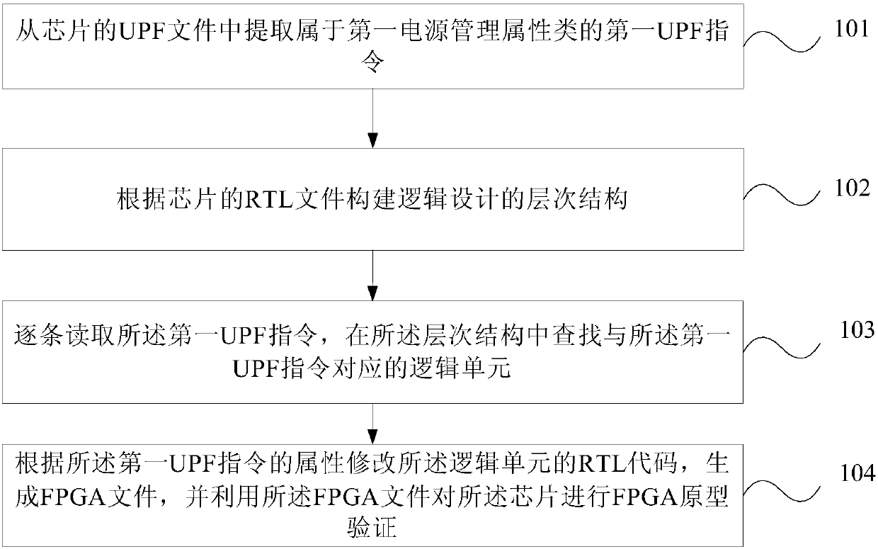
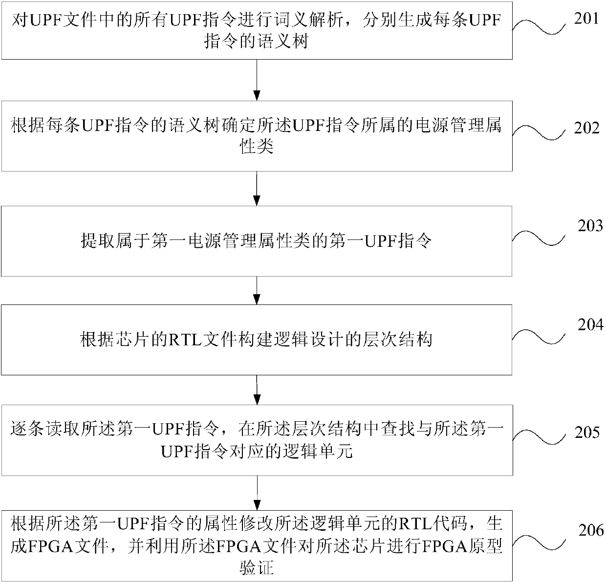
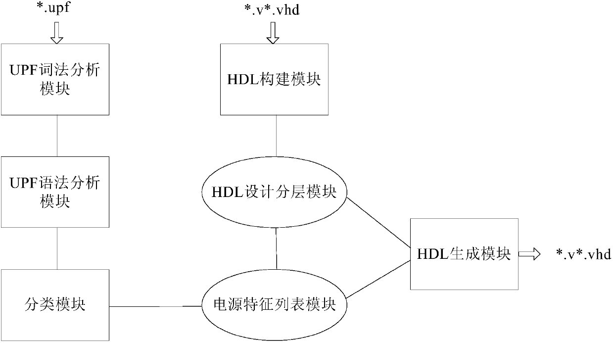
[0020] In order to make the purpose, technical solutions and advantages of the embodiments of the present invention clearer, the technical solutions in the embodiments of the present invention will be clearly and completely described below in conjunction with the drawings in the embodiments of the present invention. Obviously, the described embodiments It is a part of embodiments of the present invention, but not all embodiments. Based on the embodiments of the present invention, all other embodiments obtained by persons of ordinary skill in the art without creative efforts fall within the protection scope of the present invention.

[0021] The low power consumption design of the integrated circuit of the chip is mainly reflected in the reduction of static power consumption and dynamic flip rate. Among them, reducing static power consumption can be achieved by reducing the power supply voltage, turning off the power supply, and using high-threshold transistors. Reducing the d...


PUM


Abstract

The embodiment of the invention provides a method and a device of FPGA (Field-Programmable Gate Array) prototype verification on a chip. The method of FPGA prototype verification on the chip of the invention includes: extracting first UPF (Unified Power Format) instructions, which belong to a first power management attribute class, from a UPF file of the chip; constructing a hierarchical structureof logic design according to an RTL (Register Transfer Level) file of the chip; reading the first UPF instructions one by one, and finding logic units, which correspond to the first UPF instructions,in the hierarchical structure; and modifying RTL code of the logic units according to attributes of the first UPF instructions, generating an FPGA file, and utilizing the FPGA file for FPGA prototypeverification on the chip. According to the embodiment of the invention, power management behaviors in an integrated circuit (IC) can be simulated on a conventional FPGA, logic behaviors of the FPGA are enabled to be consistent with the integrated circuit, and a valid reference basis is provided for chip design.

Description

technical field [0001] Embodiments of the present invention relate to electronic technology, and in particular to a method and device for performing FPGA prototype verification on a chip. Background technique [0002] With the rapid development of computer technology and microelectronic technology, the application fields of chips are becoming more and more extensive. A chip is a silicon chip containing an integrated circuit (Integrated Circuit, referred to as IC), which is very small and is often a part of a computer or other electronic equipment. Among them, an integrated circuit is a circuit with a specific function that integrates a certain number of commonly used electronic components, such as resistors, capacitors, transistors, etc., and the wiring between the above-mentioned electronic components, through a semiconductor process. With the rapid development of semiconductor technology and the increase of chip operating frequency, the power consumption of the chip incre...

Claims


Application Information

Patent Timeline
Patent Type & Authority Applications(China)
IPC IPC(8): G06F17/50
Inventor 耿介
Owner HISENSE VISUAL TECH CO LTD
Why Eureka
Try Eureka