Semiconductor structure forming method
A semiconductor and isolation structure technology, applied in the field of semiconductor structure formation, can solve the problems affecting the performance of fin field effect transistors and increasing the difficulty of the process, so as to reduce the impact, improve the performance and reduce the possible effects of damage
- Summary
- Abstract
- Description
- Claims
- Application Information
AI Technical Summary
Problems solved by technology
Method used
Image

Examples
Embodiment Construction
[0032] It can be seen from the background art that there are performance problems in the FinFET in the prior art. The reasons for its performance problems are analyzed in conjunction with the formation process of FinFETs:
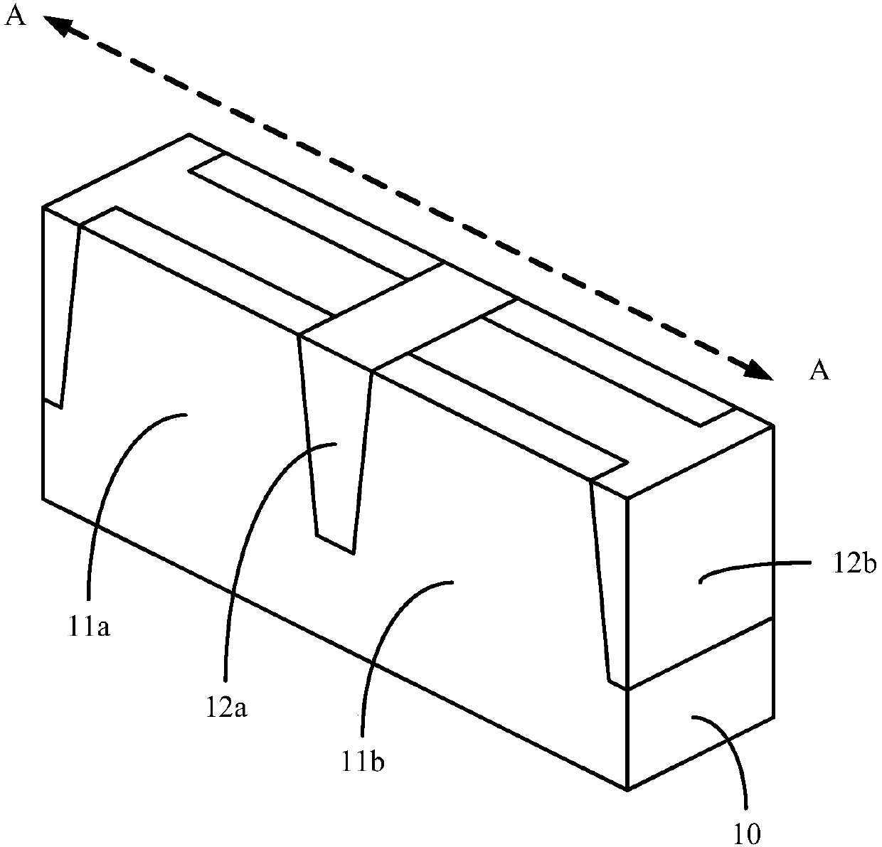
[0033] As the size of semiconductor devices shrinks, the size of transistors shrinks, and the distance between adjacent fin field effect transistors also shrinks. Stress layers of adjacent FinFETs are prone to merge, thereby causing bridging between source regions and drain regions of adjacent FinFETs. In order to prevent bridging between the source region and the drain region of adjacent FinFETs, a single diffusion break (Single diffusion break, SDB) structure is introduced in the prior art.
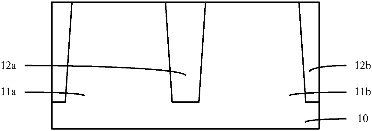
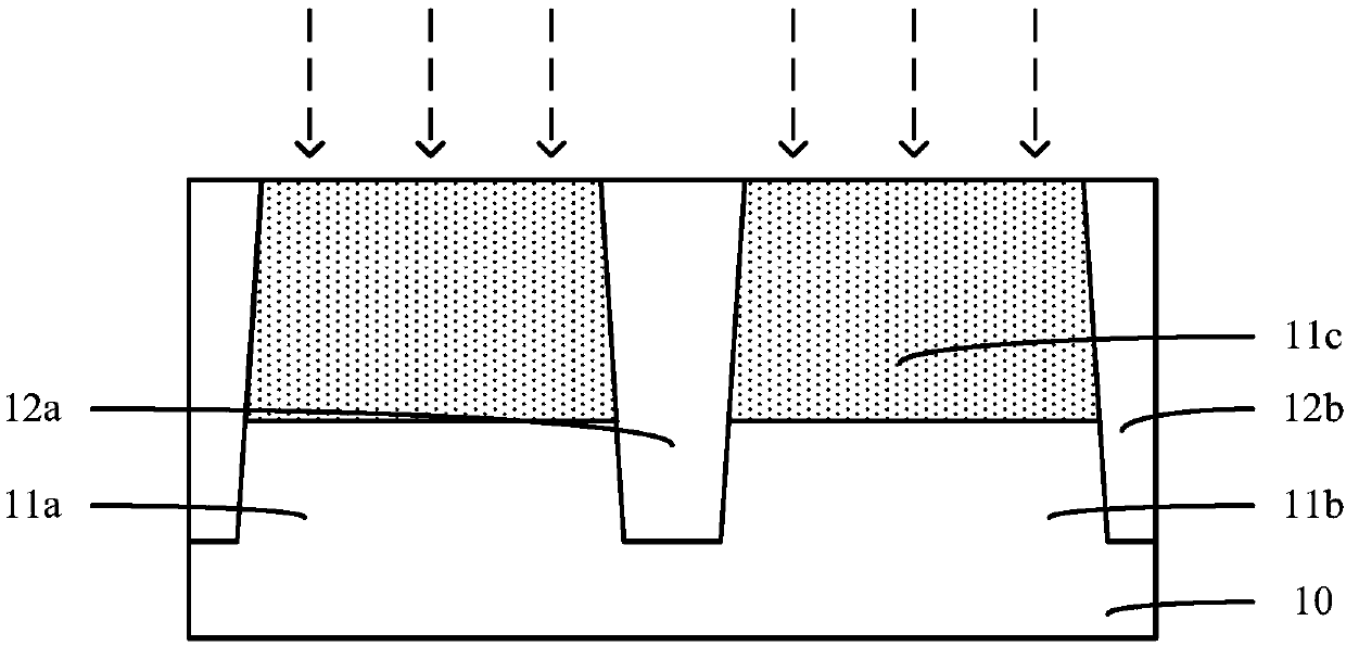
[0034] refer to Figure 1 to Figure 7 , shows a schematic diagram of a cross-sectional structure corresponding to each step of a method for forming a semiconductor structure.
[0035] refer to figure 1 and figure 2 ,in figure 2 yes figure 1 Schematic diagra...
PUM
 Abstract
Description
Claims
Application Information
 - Generate Ideas
- Intellectual Property
- Life Sciences
- Materials
- Tech Scout
- Unparalleled Data Quality
- Higher Quality Content
- 60% Fewer Hallucinations
Browse by: Latest US Patents, China's latest patents, Technical Efficacy Thesaurus, Application Domain, Technology Topic, Popular Technical Reports.
© 2025 PatSnap. All rights reserved.Legal|Privacy policy|Modern Slavery Act Transparency Statement|Sitemap|About US| Contact US: help@patsnap.com