Switching power supply module and packaging method thereof

A technology of switching power supply and switching power supply chip, which is applied in the direction of transformer/inductor coil/winding/connection, circuit, electrical components, etc. It can solve the problem of large packaging area, large power inductor, and reducing the overall power density of switching power supply modules, etc. problem, to achieve the effect of high power density, good electrical performance, and high power supply

Pending Publication Date: 2018-03-16
SHENZHEN SUNLORD ELECTRONICS
View PDF8 Cites 1 Cited by
  • Summary
  • Abstract
  • Description
  • Claims
  • Application Information

AI Technical Summary

Problems solved by technology

[0003] Most of the packaging methods of current switching power supply modules are discrete packaging, that is, peripheral components such as DC-DC chips and inductors are soldered to different positions on the pads and then packaged together. Due to the generally large volume of power inductors, the overall packaging The area is very large, which reduces the overall power density of the switching power supply module

Method used


Image

  • Switching power supply module and packaging method thereof
  • Switching power supply module and packaging method thereof
  • Switching power supply module and packaging method thereof

Examples


Embodiment Construction

[0017] The present invention will be further described below in conjunction with the accompanying drawings and specific embodiments.

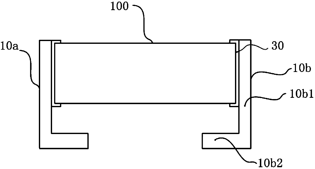
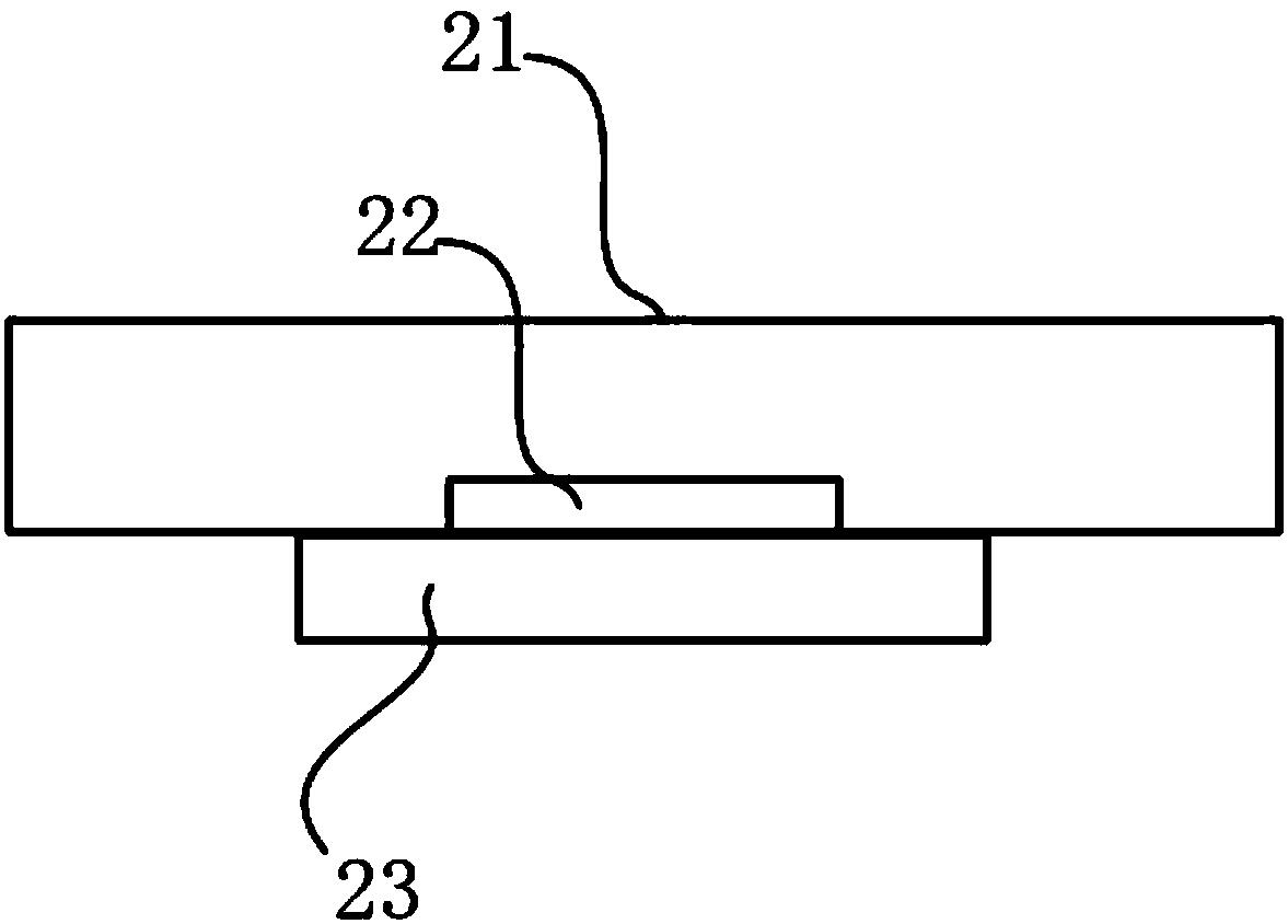
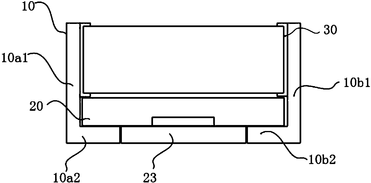
[0018] The specific embodiment of the present invention provides an integrated package switching power supply module, such as image 3 As shown, the switching power supply module includes a power inductor 10 and a switching power supply chip 20 . like figure 1 As shown, the power inductor 10 includes a magnetic core 100 and L-shaped metal terminal electrodes 10a, 10b welded to both ends of the magnetic core 100; figure 2 As shown, the switching power supply chip 20 includes a package body 21 , a bare chip 22 in the package body, and a bottom pad 23 of the bare chip. The two L-shaped metal terminal electrodes are the same, and one of them is taken as an example for illustration: the L-shaped metal terminal electrode 10b is composed of a first electrode part 10b1 and a second electrode part 10b2 perpendicular to each other, and the first elect...


PUM

PropertyMeasurementUnit
thicknessaaaaaaaaaa
sizeaaaaaaaaaa

Abstract

The invention discloses a switching power supply module and a packaging method thereof. The switching power supply module includes a power inductor and a switching power supply chip. The power inductor includes a magnetic core and L-type metal end electrodes welded to the two ends of the magnetic core. The switching power supply chip includes a packaging body, a bare chip inside the packaging body, and a bottom pad of the bare chip. Each L-type metal end electrode is composed of a first electrode part and a second electrode part perpendicular to each other, wherein the first electrode part iswelded to the magnetic core and forms a right angle with the magnetic core, and the second electrode part extends in parallel from the first electrode part to the middle of the magnetic core. The barechip and the packaging body are embedded between the first and second electrode parts and the magnetic core. The bottom pad is abutted between the two second electrode parts and is insulated from thesecond electrode parts, and the welding surface of the bottom pad is flush with the welding surfaces of the second electrode parts. The packaging method is to package the power inductor with the L-type metal end electrodes and the switching power supply chip in a nesting manner.

Description

technical field [0001] The invention relates to a switching power supply module and an integral packaging method thereof. Background technique [0002] Switching power supply has the advantages of small size and high power density. With the popularization of portable electronic devices such as smartphones, sports cameras, and Bluetooth headsets, it is developing rapidly. Power density has always been the constant pursuit of the industry. [0003] Most of the packaging methods of current switching power supply modules are discrete packaging, that is, peripheral components such as DC-DC chips and inductors are soldered to different positions on the pads and then packaged together. Due to the generally large volume of power inductors, the overall packaging The area is large, thereby reducing the overall power density of the switching power supply module. [0004] The disclosure of the above background technical content is only used to assist in understanding the inventive con...

Claims


Application Information

Patent Timeline
Patent Type & Authority Applications(China)
IPC IPC(8): H01L25/16H01L23/31H01F27/24H01F27/29
CPCH01L25/16H01F27/24H01F27/292H01L23/3107H01L24/48H01L2224/48247H01L2224/45099H01L2924/00014H01L23/495H01L24/73H01L2224/48463H01L2924/30107H01F41/0233
Inventor 王文杰陆达富
Owner SHENZHEN SUNLORD ELECTRONICS
Why Eureka
Try Eureka