

Manufacturing method of SONOS memory grid electrode structure
A memory gate and manufacturing method technology, applied in the direction of electric solid-state devices, semiconductor devices, electrical components, etc., can solve the problems of unstable reliability, ONO, corrosion, etc., and achieve the effect of saving process costs and etching process steps
- Summary
- Abstract
- Description
- Claims
- Application Information
AI Technical Summary
Problems solved by technology
Method used
Image

Examples
Embodiment Construction
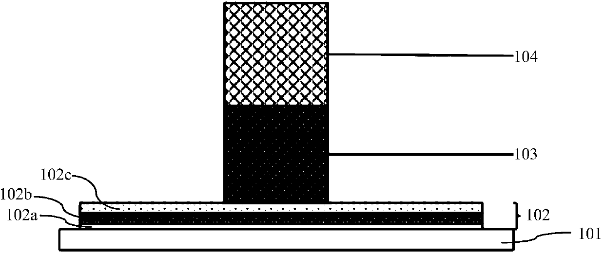
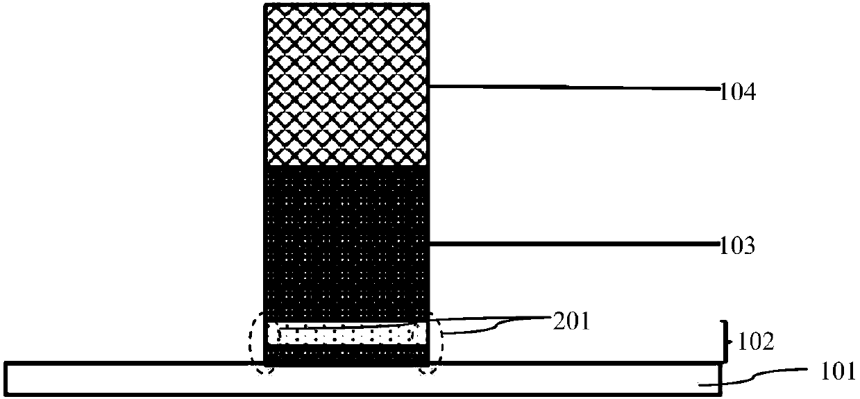
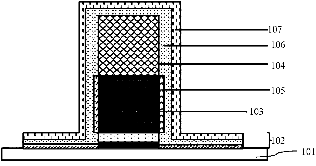
[0029] Such as figure 2 Shown is the flowchart of the manufacturing method of the SONOS memory gate structure of the embodiment of the present invention; as Figure 3A to Figure 3C Shown is a schematic diagram of the structure of each step of the manufacturing method of the SONOS memory gate structure of the embodiment of the present invention. The manufacturing method of the SONOS memory gate structure of the embodiment of the present invention includes the following steps:
[0030] Step 1, such as Figure 3A As shown, an ONO layer 2, a polysilicon gate 3, and a top oxide layer 4 are sequentially formed on the surface of a semiconductor substrate 1; the ONO layer 2 includes a first oxide layer 2a, a second nitrogen oxide layer, and oxide layer 2b and third oxide layer 2c. Preferably, the semiconductor substrate 1 is a silicon substrate. The first oxide layer 2a, the third oxide layer 2c, the subsequent top oxide layer 4 and the first sidewall oxide layer 6 are all silicon...
PUM
 Abstract
Description
Claims
Application Information