
Method for regulating threshold voltage of complementary metal oxide semiconductor

An oxide semiconductor and threshold voltage technology, which is applied in semiconductor/solid-state device manufacturing, circuits, electrical components, etc., can solve the problems of process cost reduction, unstable production, and high production cost of VTPMASK, and achieve the effect of saving process cost

Active Publication Date: 2010-06-30
FOUNDER MICROELECTRONICS INT
View PDF0 Cites 6 Cited by
  • Summary
  • Abstract
  • Description
  • Claims
  • Application Information

AI Technical Summary

Problems solved by technology

This method is suitable for the manufacturing process that product design requires VT, but according to this method, a layer of VTP MASK needs to be added separately. Due to the high production cost of VTP MASK, making VTP MASK alone is not conducive to the reduction of the entire process cost
Moreover, this method cannot meet the manufacturing process that requires a low threshold value for VTN. For example, a product design requires VTN to be 0.8V, VTP to be -0.7V, and Gate oxide (gate oxide) thickness to be 1000 angstroms. According to this requirement, the first time The dose of implanted boron ions should be 0.4E11, because the implant dose is too small and has exceeded the limit of the implanter, so stable production cannot be achieved

Method used


Image

  • Method for regulating threshold voltage of complementary metal oxide semiconductor
  • Method for regulating threshold voltage of complementary metal oxide semiconductor
  • Method for regulating threshold voltage of complementary metal oxide semiconductor

Examples


Embodiment Construction

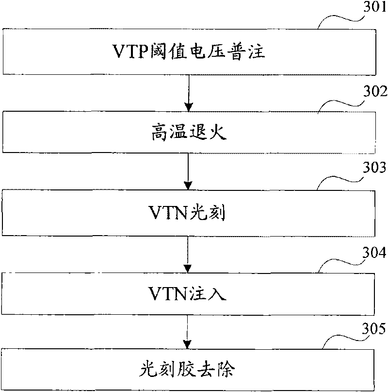
[0016] In order to accurately adjust the threshold voltage of CMOS (that is, VTN and VTP), and achieve the purpose of saving process costs, the embodiment of the present invention proposes a method for adjusting the threshold voltage of complementary metal oxide semiconductors. The following describes the present invention in conjunction with the accompanying drawings. The main realization principles of the embodiment, the specific implementation process and the corresponding beneficial effects that can be achieved are described in detail.

[0017] In the embodiment of the present invention, the silicon wafer (primary material sheet) used is an N-type silicon substrate. In the specific process flow, firstly, the N-type silicon substrate is subjected to P well photolithography through Pwell MASK (P well photolithography plate), and the Exit the P well implantation region, complete the well region implantation and advance, and form the well region; then define the source and drai...


PUM


Abstract

The invention discloses a method for regulating the threshold voltage of a complementary metal oxide semiconductor. The method mainly comprises that the implantation dosage and the energy of P-type ions are determined according the threshold value VTP of P-type metal oxide semiconductor, and P-type ion common implantation is conducted to a silicon wafer with gate oxide layer according to the result of the determination; and the implantation dosage and the energy of N-type ions are determined according to the threshold voltage VTN of N-type metal oxide semiconductor, the implantation dosage and the energy of the P-type ions, and photoetching and N-type ion implantation are conducted to the silicon wafer underwent the P-type ion common implantation according to the result of the determination and a P-well photoglyphy used to conduct P-well photoetching to the silicon wafer. By adopting the technical scheme, the VTP and the VTN can be accurately adjusted and the technological cost is saved.

Description

technical field [0001] The invention belongs to the technical field of semiconductor chip manufacturing technology, and in particular relates to a method for adjusting the threshold voltage of complementary metal oxide semiconductors. Background technique [0002] VT (Threshold Voltage, threshold voltage or turn-on voltage) is the gate voltage required to start a conductive channel between the source S and the drain D, which is for CMOS (Complementary Metal-Oxide Semiconductor, Complementary Metal-Oxide Semiconductor) It is a very important electrical parameter, especially for the currently widely used Metal Gate CMOS (Metal Gate CMOS), the threshold voltage affects the process level. Generally, the more advanced the process, the smaller the threshold voltage required to be achieved. [0003] In the traditional semiconductor chip manufacturing process, there are two main methods of adjusting VT as follows: [0004] The first method is to do one-time implantation of boron io...

Claims


Application Information

Patent Timeline
IPC IPC(8): H01L21/8238
Inventor 李如东谭志辉谭灿建
Owner FOUNDER MICROELECTRONICS INT
Learn More