Small-sized double-trapped-wave ultra-wideband antenna

An ultra-wideband antenna and dual-notch technology, applied in the field of small double-notch ultra-wideband antennas, can solve the problems of complex structure, wide notch band, interference, etc., and achieve the effects of small size, low cost and novel structure

Pending Publication Date: 2018-03-23
HEBEI UNIV OF TECH
View PDF1 Cites 1 Cited by
  • Summary
  • Abstract
  • Description
  • Claims
  • Application Information

AI Technical Summary

Problems solved by technology

For example, Hefilia Asokan proposed a new type of ultra-wideband antenna in the paper "Inductive loaded compact monopole antenna for ultra-wideband applications", which uses three monopole patches connected by lumped inductance and successfully realizes An ultra-wideband antenna that can work in the 2.85GHz1-10.6GHz frequency range; the patent publication number is CN106935967A discloses a miniaturized double-notch UWB antenna based on EBG. The antenna uses an EBG structure, and its working bandwidth is 3GHz-12GHz, and There is a notch band at 5.5GHz, but these antennas still have problems such as being susceptible to interference from WIMAX signals at 3.5GHz and wireless LAN signals at 5.5GHz, complex structures, and wide notch bands.

Method used


Image

  • Small-sized double-trapped-wave ultra-wideband antenna
  • Small-sized double-trapped-wave ultra-wideband antenna
  • Small-sized double-trapped-wave ultra-wideband antenna

Examples


Embodiment 1

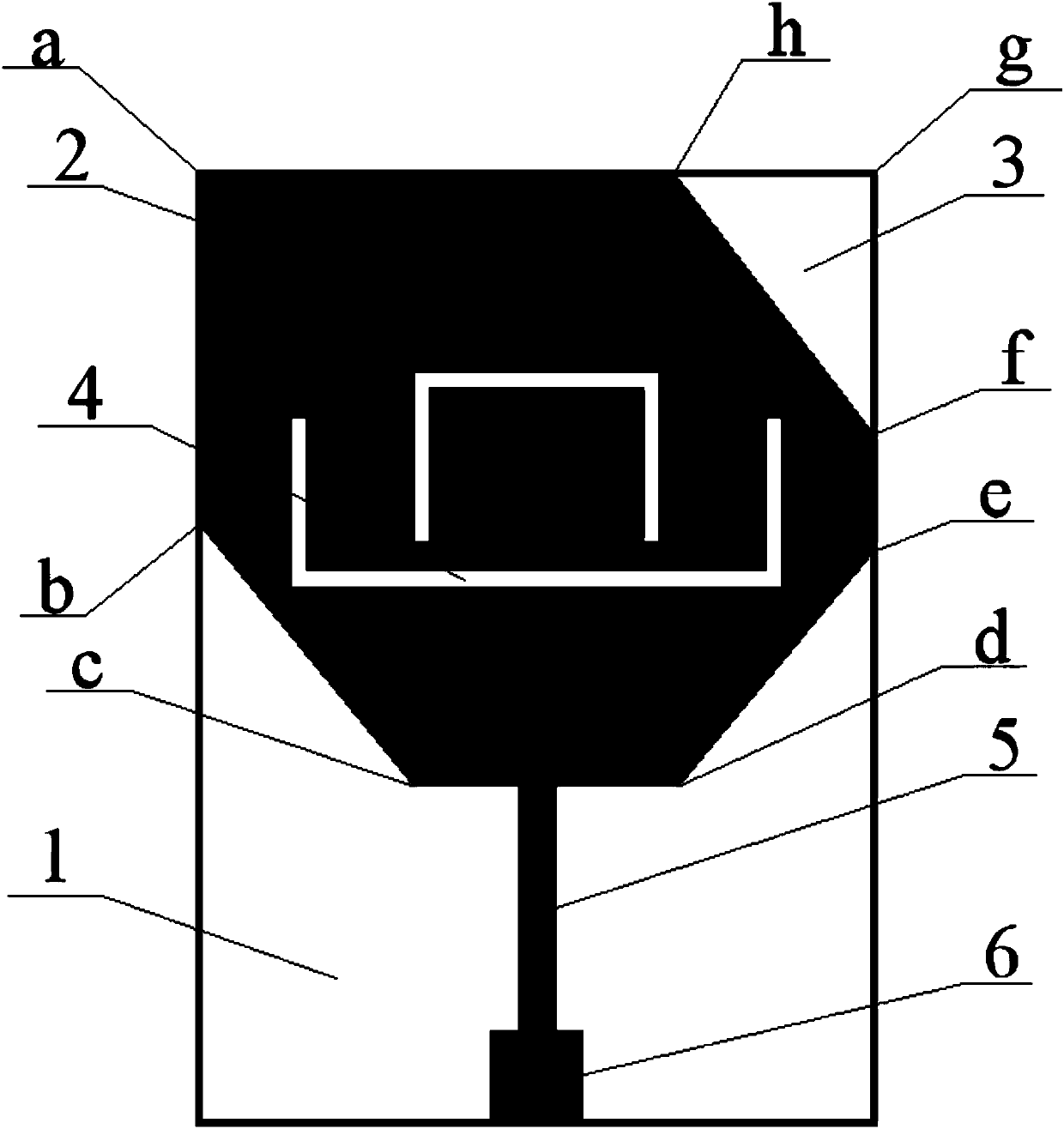
[0027] The small double-notch ultra-wideband antenna of this embodiment includes a dielectric substrate 1, a radiation unit 2, a microstrip feeder 6, an impedance matcher 5, and a ground plane 7. The back side of the dielectric substrate is printed with a ground plane, and the ground plane is on the back side of the dielectric substrate At the bottom, the radiating unit and the microstrip feeder are printed on the front of the dielectric substrate, the impedance matcher is printed on the front of the dielectric substrate, the radiating unit is connected to the impedance matcher, the impedance matcher is connected to the microstrip feeder, and the radiating unit is in the dielectric On the top of the front side of the substrate, the impedance matcher is directly below the radiating unit, and the microstrip feeder is directly below the impedance matcher;

[0028] In this embodiment, the shape of the dielectric substrate 1 is rectangular, its material is polytetrafluoroethylene (F...


PUM


Abstract

The invention relates to a small-sized double-trapped-wave ultra-wideband antenna. The small-sized double-trapped-wave ultra-wideband antenna comprises a dielectric substrate, a radiating unit, an impedance matcher, a micro-strip feeder and a grounding surface. A grounding surface is printed at the bottom of the backside of the dielectric substrate; the radiating unit, the impedance matcher and the micro-strip feeder are printed at the front side of the dielectric substrate; the radiating unit is connected with the impedance matcher; the impedance matcher is connected with the micro-strip feeder; the radiating unit is at the top part of the front side of the dielectric substrate; the impedance matcher is under the radiating unit; the micro-strip feeder is under the impedance matcher; the radiating unit is a polygon which is formed by cutting off right-angle triangles at the lower left, lower right and upper right of a rectangle; two C-shaped grooves are formed in the middle of the radiating unit; the impedance matcher is rectangular; and the two C-shaped grooves are distributed symmetrically by regarding the beeline where the impedance matcher is as an axis. The antenna has two trapped wavebands at 3.5 GHz and 5.5 GHz, and can efficiently remove interference from global microwave interconnection access signals at 3.5 GHz and wireless local area network signals at 5.5 GHz.

Description

technical field [0001] The invention belongs to the technical field of wireless communication, in particular to a small double-notch ultra-wideband antenna. Background technique [0002] With the rapid development of the current wireless communication system, people have higher and higher requirements for the data transmission rate in wireless communication, which also requires the bandwidth of the channel to be wider and wider, which in turn requires the working bandwidth of the antenna to be wider and wider, which makes the The working performance of broadband antennas can no longer meet people's requirements for data transmission rates in wireless communications; since the Federal Communications Commission named 3.1GHz-10.6GHz as ultra-wideband and issued a license to it, ultra-wideband antennas have attracted many researchers. attention. [0003] At present, in order to realize the ultra-wideband antenna, the monopole patch antenna technology is generally used, and this...

Claims


Application Information

Patent Timeline
IPC IPC(8): H01Q1/38H01Q1/48H01Q1/50H01Q1/52
CPCH01Q1/38H01Q1/48H01Q1/50H01Q1/52
Inventor 郑宏兴吝子祥王霞王蒙军
Owner HEBEI UNIV OF TECH
Why Eureka
Try Eureka