
Bandgap reference circuit for implementing high-order temperature compensation of diode by means of MOS transistor

A high-order temperature compensation and reference circuit technology, applied in the field of microelectronics, can solve problems such as application limitations

Active Publication Date: 2018-03-30
CHONGQING UNIV OF POSTS & TELECOMM
View PDF10 Cites 10 Cited by
  • Summary
  • Abstract
  • Description
  • Claims
  • Application Information

AI Technical Summary

Problems solved by technology

Since V EB1 Due to its non-linearity, the output voltage of the traditional first-order bandgap reference circuit has the disadvantage of high temperature coefficient, so the application of the traditional first-order bandgap reference circuit in high-precision systems is greatly limited

Method used


Image

  • Bandgap reference circuit for implementing high-order temperature compensation of diode by means of MOS transistor
  • Bandgap reference circuit for implementing high-order temperature compensation of diode by means of MOS transistor
  • Bandgap reference circuit for implementing high-order temperature compensation of diode by means of MOS transistor

Examples


Embodiment

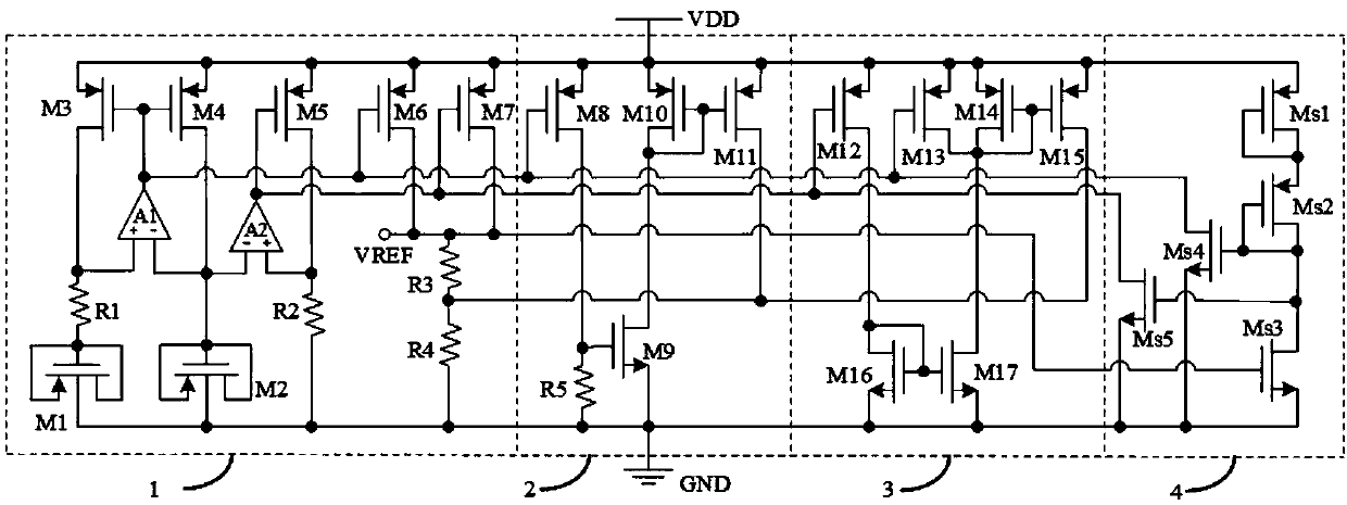
[0029] A high-order temperature-compensated bandgap reference circuit for implementing a diode with a MOS tube, such as figure 2 As shown, it includes a first-order bandgap reference circuit 1, a temperature curvature compensation circuit 2 in a high temperature region, a segmented temperature compensation circuit 3 in a low temperature region, and a start-up circuit 4;

[0030] Wherein the starting signal output end of the starting circuit 4 is respectively connected to the starting signal input ends of the first-order bandgap reference circuit 1, the high temperature region temperature curvature compensation circuit 2 and the low temperature region temperature section compensation circuit 3, so The signal output terminals of the first-order bandgap reference circuit 1 are respectively connected to the signal input terminals of the high-temperature region temperature curvature compensation circuit 2 and the low-temperature region temperature segment compensation circuit 3, an...


PUM


Abstract

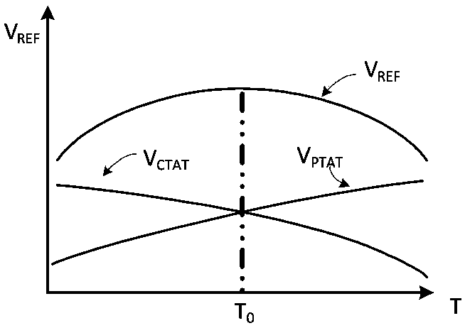
The present invention discloses a bandgap reference circuit for implementing the high-order temperature compensation of a diode by means of an MOS transistor. The bandgap reference circuit comprises afirst-order bandgap reference circuit, a high-temperature region temperature curvature compensation circuit, a low-temperature region temperature segment compensation circuit and a startup circuit. According to the bandgap reference circuit, a drain electrode and a substrate of a PMOS transistor in which a source electrode, the drain electrode and a gate electrode are in short connection with oneanother form a forward end and a reverse end of the diode respectively; by utilizing negative temperature coefficient voltage VCTAT generated by the drain-substrate voltage of the PMOS transistor inwhich the source electrode, the drain electrode and the gate electrode are in short connection with one another and positive temperature coefficient voltage VPTAT generated by the difference of two drain-substrate voltages of the PMOS transistor in which the source electrode, the drain electrode and the gate electrode are in short connection with one another, the negative temperature coefficient voltage VCTAT and the positive temperature coefficient voltage VPTAT are weighted to obtain first-order bandgap reference voltage, high-temperature region temperature curvature compensation voltage VNL1 and low-temperature region temperature segment compensation voltage VNL2 are introduced to the first-order bandgap reference circuit to obtain bandgap reference voltage with a low-temperature coefficient, and therefore the bandgap reference circuit for implementing the high-order temperature compensation of the diode by means of the MOS transistor is obtained.

Description

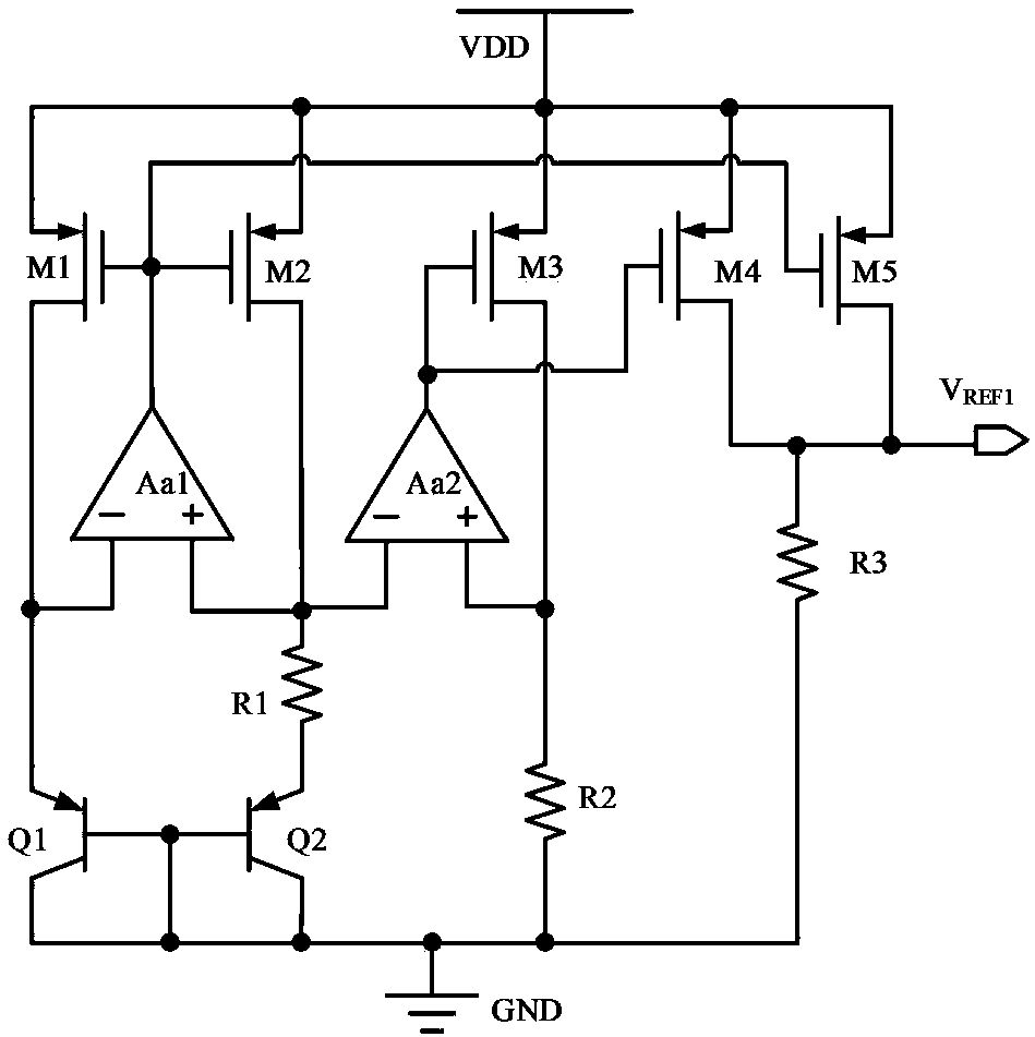
technical field [0001] The invention belongs to the technical field of microelectronics, and in particular relates to a high-order temperature compensation bandgap reference circuit realized by a MOS transistor for a diode. Background technique [0002] The bandgap reference circuit is an important module of modern analog integrated circuits and digital-analog hybrid integrated circuits, and its performance characteristics directly affect the performance of the entire circuit, which requires improving the performance characteristics of the bandgap reference circuit. [0003] figure 1 It is a basic CMOS bandgap reference circuit structure, and its basic idea is to use the emitter-base voltage V of the PNP transistor Q1 with negative temperature characteristics EB1 It is weighted with the difference between the emitter-base voltages of two PNP transistors with positive temperature characteristics to obtain a reference voltage with zero temperature characteristics. The resist...

Claims


Application Information

Patent Timeline
IPC IPC(8): G05F1/567
CPCG05F1/567
Inventor 周前能徐海峰李红娟关晶晶程飞鸿郭涛林金朝李国权
Owner CHONGQING UNIV OF POSTS & TELECOMM
Learn More