Low-voltage low-power consumption CMOS voltage reference circuit
A voltage reference and reference circuit technology, applied in the direction of adjusting electrical variables, instruments, control/regulation systems, etc., can solve the problems of increasing circuit area and reducing reference circuit speed, achieving low power consumption and cost, reducing area, The effect of high integration
- Summary
- Abstract
- Description
- Claims
- Application Information
AI Technical Summary
Problems solved by technology
Method used
Image
Examples
Embodiment Construction
[0042] In order to make the object, technical solution and advantages of the present invention clearer, the present invention will be described in further detail below in conjunction with specific embodiments and with reference to the accompanying drawings.
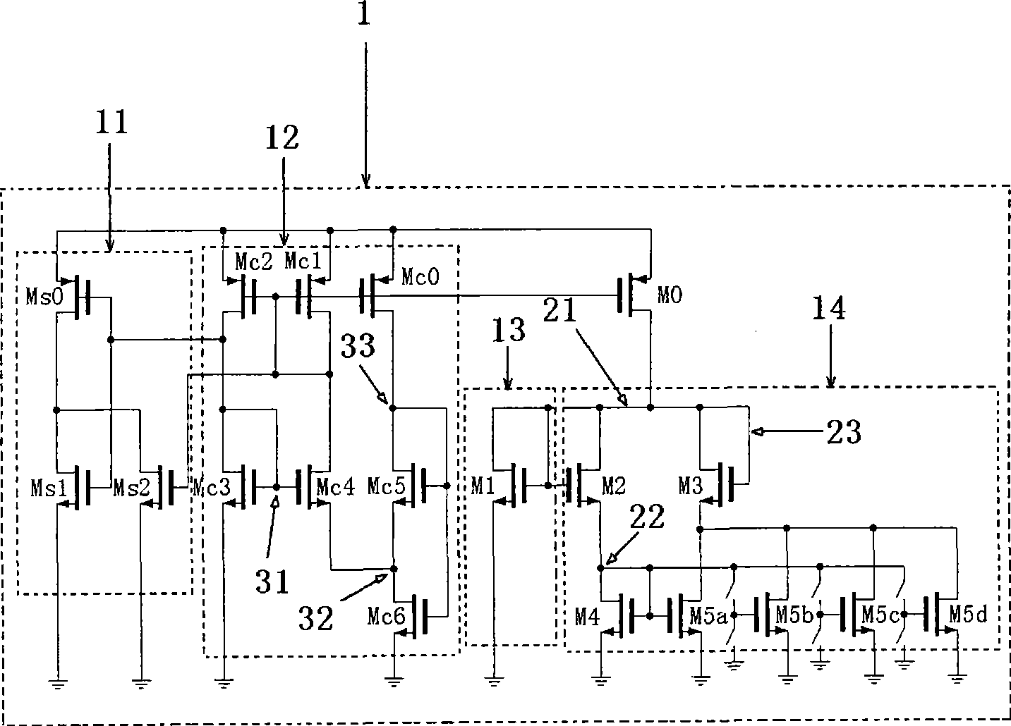
[0043] Such as figure 1 as shown, figure 1 It is a circuit diagram of a low-voltage low-power consumption voltage reference circuit according to the present invention, and the CMOS voltage reference circuit includes a start-up circuit 11, a self-bias current source 12, a voltage generator 13 with a negative temperature coefficient, and a reference voltage regulator device 14, and a single-tube current mirror MOS transistor M 0 .
[0044] Wherein, the start-up circuit 11 is composed of a transistor M S0 , M S1 and M S2 constitute; among them, the PMOS transistor M S0 and NMOS transistor M S1 form a basic inverter cell, M S0 , M S1 The drain and gate of the transistor are respectively connected, and the source is r...
PUM
 Abstract
Description
Claims
Application Information


